
The study of micro and nano surface metrology is becoming commonplace in industrial and research environments as structures and surface features become smaller and smaller. One area where this is evident is the expansion of interest in noncontact metrology for measurement of different types of microelectromechanical systems (MEMS) structure.
Scanning interferometry is becoming increasingly important in the analysis of MEMS devices because of a variety of factors including:
It can address many of the challenging measurement problems that exist when studying MEMS structures. These include solving etch rate/time problems, measuring stress gradients, elastic properties, the measurement of critical dimensions, heights, angles and surface roughness.
The technique offers nano/micro height measurements and sub-micro/micro/millimeter lateral measurements with high spatial resolution. The combination of a large field of view and high lateral sampling-more than 1 million measurement points-allows it to offer a broad range of measured bandwidths for a single measurement.
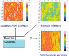
Thin film data is obtained from a single measurement. Source: Ametek Taylor Hobson
Theory of Optical Interferometry
The use of optical techniques to study surfaces has been popular for a long time and there have been many developments over the years to improve the accuracy of the metrology.Interferometry has now become an important metrology tool due the introduction of modern electronics, computers and software to the basic technique. Typically there are two different modes commonly used, phase shifting and vertical scanning.
Phase-shifting interferometry has proven to be powerful and many commercial interferometers use phase-shifting techniques. The technique involves measuring the phase shift as the sample or optics are scanned in Z. While phase-shifting interferometry has great precision, it has limited dynamic range.
It can easily be shown that for phase-shifting interferometry the height difference between two adjacent data points must be less than λ/4, where λ is the wavelength of the light used. If the slope is greater than λ/4 per detector pixel, then height ambiguities of multiples of half wavelengths exist.
For example, if the light source has a wavelength of 633 nanometers then the maximum step that can be measured is 633/4 = 158.25 nanometers. In order to overcome this limitation, scanning interferometry is often used. Scanning interferometry is more suited to the measurement of MEMS devices because it had a much greater Z range than phase shifting and modern algorithms such as those used in coherence correlation interferometry are able to match the precision of phase shifting over the much longer range.
A schematic of a scanning interferometer system is shown in figure 1. The upper beam splitter directs light from the light source toward the objective lens. The lower beam splitter in the objective lens splits the light into two separate beams. One beam is directed toward the sample and one beam is directed toward an internal reference mirror. The two beams recombine and the recombined light is sent to the detector. When the path length to the sample and the reference are the same, interference is observed. The detector measures the intensity as the interferometric objective is scanned in Z.
The detector takes a series of snapshots as the sample is measured. This gives a series of images of the intensity map of the light being reflected from the surface. The area of interest for the measurement is the interference area. These intensity images are used to create a 3-D image of the surface being measured.
Different techniques are used to control the movement of the interferometer and also to calculate the surface parameters. The accuracy and repeatability of the scanning white light measurement are dependent on the control of the scanning mechanism and the calculation of the surface properties from the interference data.
Step Height Measurements
Scanning interferometry is a powerful technique for the measurement of step heights. The subnanometer vertical resolution and high spatial resolution lead to a highly detailed 3-D representation of the specimen under test. This 3-D information can be used to obtain accurate and repeatable step height information. The added advantage of a full 3-D representation of the surface is the ability to measure the whole of the step and look for any variation in step height along the step edge.One of the recent advances in step height measurement is the ability to obtain accurate step height and roughness in a single measurement. Previously the measurement of large step heights involved long measurement times or high-speed measurement at lower Z resolution.
The advent of long range closed-loop scanners means that it is now possible to use Z stitching to accurately measure the surface of the bottom step and then move to the top surface and accurately measure the surface at the top of the step. The two measurements can then be combined to give an accurate step height measurement and subnanometer roughness measurement.
Roughness Measurements
Roughness is an important parameter for the control of the sample properties. Various roughness ranges are normally studied in order to define the overall properties of the surface and one of the limitations to the analysis is the bandwidth of the measurement method.Varying the size of the field of view makes comparison of datasets difficult because it normally involves changing the pixel size and it is not trivial to compare roughness data with varying pixel sizes. The X, Y bandwidth of interferometry measurements is normally restricted by the field of view of the optics used and the number of pixels of the camera. Therefore moving from a camera with 76,800 (320 x 240) pixels to a camera with more than 4 million (2,048 x 2,048) pixels leads to a large improvement in the range of roughness information that can be obtained.
Another consideration is the dimensions of the camera, some analysis require a set of data that is square so a 320 x 240 camera actually gives a dataset that has 240 x 240 usable pixels-this will give much less information than a 2,048 x 2,048 pixel camera.
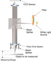
Figure 1: A typical interferometer setup Source: Ametek Taylor Hobson
Measurement of sample deformation
One of the common metrology requirements of MEMS devices is the study of the performance of difference components. This often is in the form of measurement of the deflection or deformation of part relative to another. Because of the high vertical and lateral resolution and speed of measurement, vertical scanning interferometry is ideal for these studies.The capability to measure these changes in a dynamic way had been recently introduced with the inclusion of a stroboscopic light source into the interferometer system. If the stroboscopic frequency is set to the same frequency as the sample frequency, the dynamic movement of the MEMS device can be studied by “freezing” the movement. If the phase of the stroboscopic light source is varied, the whole movement cycle of the component can be studied.
Coated surfaces
Accurate analysis of coated surfaces is important for many MEMS devices. The interferometry technique has been extended to measure the thickness of transparent and semitransparent films. Thick and thin films present some potential problems during optical measurements. The problem arises from the possibility of producing signal from different layers that can confuse the measurement and sometimes produce an incorrect answer.As the effects of films coatings on interferometry measurements are now becoming more widely understood, there is growing interest in the measurement of thin film surfaces and thin film thickness. For films with thicknesses in excess of 1 to 2 microns, the vertical scanning measurement of the film leads to a series of fringe envelopes, each fringe envelope corresponding to a surface interface. It is relatively trivial to locate the positions of these envelope maxima and therefore determine the film thickness, assuming the refractive index is known.
For thinner films the measurement leads to the formation of a single interference maxima. In this case, it is appropriate to describe the thin film structure in terms of optical admittances; this data that can be treated by the introduction of a new function, the helical conjugate field (HCF) function. This function may be considered as providing a “signature” of the multilayer measured so that through optimization, the thin film multilayer may be determined on a local scale.
Thick Film Analysis
The thickness and real surface roughness of films can be obtained by measuring a step or by measuring through the film to the substrate. Because of the l/4 limit of PSI, it is often not suitable for film thickness measurements and some form of scanning interferometry is used. Because of the high Z resolution of the coherence correlation interferometry (CCI) technique, it is an ideal technique for measuring film thickness.In CCI for thick film measurement, the optics are moved vertically so that the upper and lower film surfaces pass through focus. For each pixel a set of interference fringes are obtained during the scan: the first one corresponding to the air/film interface, and the last corresponding to the film/substrate interface. The CCI algorithm then calculates the maxima of the fringes envelopes with subnanometer resolution. The film thickness is calculated from the distance between the maxima and the refractive index of the film.
Measurement of the top surface of semitransparent surfaces also can be a problem. Normally measurement of the roughness of top surfaces of semitransparent films is complicated by the signal coming from other surfaces. If possible, the problem can be solved by setting the scan length so that only the top set of fringes are covered by the scan and the signal from the bottom set of fringes is not seen. This can be a problem if the surface is thinner than about 4 microns or if the measurement is part of an automation process.
In order to overcome this problem it is possible to instruct the software to just use the signal from the top surface alone. It also is possible to measure other surfaces by specifying which of the fringe envelopes is to be studied. Care has to be taken with the analysis of the surface apart from the top surface because the measurement data can be affected by any nonhomogeneity in the film.
For thinner films, the fringe envelopes may overlap. In this case, an intensity-based threshold can be applied to separate the two sets of fringes. This means that thicknesses less than 2 microns can be measured with the same accuracy as the thicker films shown above. However, as the fringe envelopes approach each other, they will start to deform the overall shape of the waveform and, therefore, the thin film measurement.
Thin Film Analysis
Conventionally, thin film structures are measured using either a spectrophotometer or an ellipsometer. For large-area vacuum deposited thin films (single or multilayer), there is now a growing requirement for measurement of thin film structures that only exist on a local scale. It is impossible to easily study the signal from the top of the thin film and the signal from the substrate if the film is less than about 1.5 microns because of the fringe overlap.Recent studies have shown that through the development of the HCF function, it is possible to extend coherence correlation interferometry to include the calculation of layer thicknesses from this type of sample.
An additional benefit is that through the knowledge of the thin film structure, the phase-change on reflection may be compensated so that “true” step-heights may be obtained. It can be shown that through performing coherence correlation interferometry experiments on a thin film coated substrate (single or multilayer), together with a reference substrate, such as the glass BK7 with a similar reflectivity to the film, it is possible to construct the HCF function. And from this procedure the film thickness can be calculated for films thicknesses down to about 20 nanometers.
Interfacial surface roughness
The surface roughness of a thin film sample is often a composite roughness of the top surface and the bottom surface. This can lead to large errors in the true surface roughness of the top surface. Because the HCF can be used to obtain separate information from the different layers, it can be used to analyze the surface parameters for the interfaces, including the air-top surface interface. This means that it is possible to measure the true roughness of the top surface of a thin film sample where the film thickness is greater than about 20 to 30 nanometers. It also is possible to measure the interface roughness.Scanning interferometry is a powerful tool for measuring MEMS devices. It has the ability to obtain step height, roughness and lateral dimension information from a single noncontact measurement. Other important advantages include the high speed and high repeatability of the technique. Recent developments such as long range closed loop scanners, dynamic measurements and coating analysis are increasing the usefulness of the technique.Q