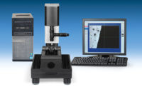
Nanometrics, a provider of advanced process control metrology solutions and inspection systems for fabrication of LEDs, semiconductors, solar photovoltaics and data storage devices has acquired Nanda Technologies of Munich, Germany.
Nanda, a provider of completely automated wafer inspection systems that are applicable for semiconductor fabrication processes has developed a novel optical defect inspection technology for manufacturing semiconductor products.
The acquisition has bolstered Nanometrics’ metrology solutions portfolio with the advanced optical technology for macro defect inspection. Nanda’s SPARK technology has the ability to capture full-wafer surface inspection images during production speeds at high volume. For most of the modern technology nodes, the SPARK technology platform enables 100% device sampling and accurate wafer inspection. It also supports different types of surface topographies and materials. The platform is aimed to address the $300 to $400 million metrology market opportunity.
Nanometrics has acquired Nanda for around $23 million in cash. This acquisition may lead to a $0.03 to $0.05 negative EPS impact during the fourth quarter, 2011, which includes operating expenses, purchase accounting charges and transaction costs. The acquisition will lead to the establishment of the SPARK team as a center for inspection technology excellence at Nanometrics. The acquisition includes intellectual property, technology assets, staff and facilities.
The president and CEO of Nanometrics, Dr. Timothy J. Stultz, stated that the acquisition expanded its served markets and will contribute to the company’s business. Nanda Technologies’ CEO, Dr. Lars Markwort, has become the Nanometrics’ Inspection business unit’s general manager. He stated that the acceptance of SPARK technology will increase due to Nanometrics’ customer relationships, international infrastructure and process control.
For more information, visitwww.nanometrics.com .
Get our new eMagazine delivered to your inbox every month.
Stay in the know with Quality’s comprehensive coverage of the manufacturing and metrology industries.
SIGN UP TODAY!Copyright ©2024. All Rights Reserved BNP Media.
Design, CMS, Hosting & Web Development :: ePublishing

