No matter what marvels emerge from their manufacturing plants, electronics assemblers never satisfy the demand for smaller, cheaper and better-performing products. Among other things, this endless demand has caused exponential growth in printed circuit board (PCB) solder connections, as well as in the number of packages with hidden solder joints. The burgeoning crop of concealed connections creates major inspection difficulties for makers of BGA, µBGA, CGA and flip-chip devices.
But there is a solution to problems posed by tough electronics-inspection tasks: high-resolution X-ray systems. These powerful systems are designed to help operators reliably assess the quality of concealed solder connections. Unlike machine vision and optical inspection equipment, X-ray systems penetrate materials to expose hidden solder joints in a variety of area array devices.
Besides their role in PCB manufacturing, X-ray systems are tackling new inspection challenges in wafer fabrication. What is more, engineers have unveiled ultra-high-resolution X-ray machines designed to spot tiny flaws in the growing ranks of micro-scale electromechanical systems.

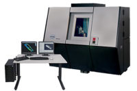
The most effective 2-D X-ray inspection systems consist of three major components: an X-ray source, which is a sealed or open tube, an X-ray detector and a fixture for holding and manipulating the part being inspected. Source: Feinfocus
Key components
The most effective 2-D X-ray inspection systems consist of three major components: an X-ray source, which is a sealed or open tube, an X-ray detector, and a fixture for holding and manipulating the part being inspected. Open microfocus tubes normally are used to meet the high-resolution requirements of electronics assembly and packaging. As the name suggests, micro-focus tubes can provide spatial resolution down to 1 micrometer. Resolution depends on the size of the focal spot, or the focus-the area within the tube head that emits the X-ray beam.The detector gathers the X-ray waves traveling through the sample and processes the information in real-time to produce a visible image that can be assessed by the human eye. The most common detector is a combination of video camera and image intensifier that converts X-rays into visible light. New detector options include high-dynamic cameras and flat panel direct digital detectors.
The manipulator is used for precise X-Y-Z positioning, and rotation and tilting of the sample. The device should be able to vary directional and rotational speeds for requirements ranging from quick overview searches at low magnification to very low speed inspections at high magnification.

There are three different ways to achieve oblique viewing, from left to right: conventional, advanced and close-to-focus oblique viewing inspection with AIM Technology. Source: Feinfocus
Views at an angle
A sophisticated manipulation system is a key component of advanced 2-D X-ray inspection systems. 2-D inspection equipment that cannot tilt and rotate the sample limits the operator to top-down views of the sample. But top-down views usually are insufficient for a thorough assessment of the solder connections in today's electronic devices. Manufacturers must also inspect the third dimension of solder joints to be certain they have not overlooked any defects.A 3-D imaging system can provide the necessary inspection data. But 3-D analysis can take longer than a 2-D inspection, slowing down PCB production. A faster alternative is a 2-D system that tilts and rotates samples at oblique angles to the X-ray beam. This oblique viewing technique provides a look at the critical third dimension, allowing operators to check parts from multiple orientations.
But not all oblique viewing systems offer the best inspection solution. Some only provide views from certain angles or rotational positions. Furthermore, for an increasing number of applications, the oblique views provided by tilting and rotating the sample fail to produce the required magnification because the sample automatically tilts away from the focal spot when using this system setup for off-axis inspections. To enable oblique views at highest magnifications, manufacturers need a close-to-focus oblique inspection. As the name suggests, this involves positioning the sample as close as possible to the focal spot while still allowing oblique views.
In addition, many systems require highly skilled operators to keep the region of interest in the machine's field of view during complex inspection routines that require movement of the sample, the detector or both.
AIM advantage
These physical and practical considerations provided the impetus for Auto Isocentric Motion (AIM) technology. An AIM-equipped oblique-viewing system allows for close-to-focus inspection and provides sharp, intricate sample views from any angle or rotational position. In an AIM-driven system, the X-ray detector can be moved in various directions while the sample stays flat and close to the focal spot. For this purpose, the detector is mounted on a special curved guide that allows tilt up to 60 degrees off-axis. This guide sits atop a rotational pivot that permits a full 360-degree rotation. The detector can stop at any point on the resulting "dome of motion," while maintaining a constant distance from the X-ray source.X-rays are emitted from the focal spot in a conical pattern. Positioned in the center of the dome of inspection, the detector gathers X-rays from the center of the cone. By moving the detector away from the dome center, the operator shifts the viewing line, allowing the device to gather X-rays from the outside edges of the cone. A precondition for this convenient procedure is the use of an open microfocus tube of the transmission target type, which provides a total cone angle of 170 degrees and a minimum focus-to-object distance of 0.25 millimeter.
With every move of the detector, AIM automatically keeps the area to be X-rayed, or region of interest, within the system's field of view. The keys to AIM's automatic adjustments are precise manipulator technology and sophisticated algorithms that compute the manipulator movements, keeping the region of interest in the viewing line.
Another important aspect of an AIM-driven oblique-viewing system is the system's ability to perform complex manipulations without the risk of sample damage. Because of sophisticated anticollision protection, operators can focus on the images produced by the system with no worries about sample position or collisions. Unlike other software-driven anticollision features that require the operator to enter anticollision specs into the program, the integrated anticollision protection is 100% automatic. An optical camera image snapshot of the loaded sample tray scene serves as a map for quick positioning of the manipulator.
To help operators with this task, an AIM-driven system offers a variety of image manipulation and processing tools. These include: Click and Center, which brings the area of interest into center view; Frame and Zoom, which magnifies the area of interest until it fills the screen; Tilt and Rotate, which uses onscreen virtual joysticks to re-position the detector while keeping the region of interest in view; and Tilt and Circle, which allows real-time rotating views of the region of interest at any magnification and at any angle. All operations can be performed with a mouse click.
System capabilities also include real-time image processing characteristics such as contrast enhancement, edge outline, background subtraction and pseudo 3-D representation. These features help to provide operators with the best possible images on which to base pass-fail decisions. In addition, the system includes Automatic Defect Recognition such as automatic voiding calculation and solder joint measurement and analysis. AIM-equipped oblique-viewing systems are recommended for multi-layered parts that are difficult and time-consuming to inspect with conventional systems.

The Conical Target positions the focal spot at the end of a cone-shaped tube head. Source: Feinfocus
A closer look
For a more flexible lab setup with versatile sample tilt and rotate manipulation without AIM technology, effective close-to-focus inspections can be performed with the help of a Conical Target, a technology that positions the focal spot at the tip of a cone-shaped tube head. This optional feature is easily mounted on a standard transmission X-ray tube without any additional tools. The device's conical shape lets operators move the focal spot between actual components on a populated board.In addition to PCB manufacturing plants, 2-D X-ray inspection systems are finding a home in semiconductor fabrication and packaging facilities. For years, these facilities have relied on optical, laser and UV inspection tools to detect surface defects, such as pits, nodules, scratches and contaminants. With the advent of wafer bumping technology, conventional wafer defect detection techniques have been employed to check bump volume parameters, such as diameter, height and roundness. Because they cannot determine the amount of true solder mass, conventional techniques are unable to gage soldered product reliability and performance. So wafer facilities are turning to high-resolution X-ray inspection, the only technique that can analyze solder mass and spot voids hidden beneath the surface of a bump. In these settings, the most effective X-ray inspection systems are tailored to meet regulatory automated handling standards for 200-millimeter and 300-millimeter wafer capability.

The WBI-FOX X-ray inspection system has been tailored to meet regulatory automated handling standards for 200-millimeter and 300-millimeter wafer capability. Source: Feinfocus
Need for nanofocus
Despite their impressive capabilities, microfocus X-ray devices were not designed to meet the unique inspection challenges posed by micro-electromechanical systems (MEMS) and micro-opto-electromechanical systems (MOEMS). The emergence of MEMS and MOEMS has been a driving force behind the development of so-called nanofocus X-ray technology. With a focal spot of less than 1 micrometer in diameter, nanofocus systems can provide the detail and resolution required to inspect ultra-small components. Even when an application does not require nanofocus technology, the extremely high resolution produces a sharper image of the inspection area.Two-dimensional microfocus X-ray inspection systems penetrate materials to help PCB manufacturers assess the quality of hidden solder connections in area array devices. Thanks to some clever technological advances, these 2-D systems can provide a look at the critical third dimension without slowing down PCB production lines. X-ray systems also are taking on tough inspection tasks in semiconductor manufacture. In MEMS and MOEMS production, new nanofocus X-ray machines produce ultra-high-resolution images that can identify the tiniest of defects. Some X-ray systems combine microfocus, nanofocus and high-power capabilities, giving manufacturers the flexibility to match the X-ray mode to the inspection task at hand.
Dr. Udo E. Frank has served as director of technology development for Feinfocus. Dr. Norbert Daneke is an X-ray physical engineer with Feinfocus. They can be contacted at [email protected]

