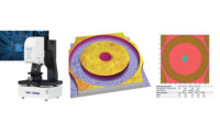
Semiconductor test equipment supplier Advantest and Digital Surf announced that PM3D Map software based on Digital Surf’s industry-standard Mountains Technology® is now incorporated into the company’s Multi Vision Metrology Scanning Electron Microscope (MVM-SEM®) series. Advantest’s MVM-SEM® system together with PM3D Map software now provide a complete solution for measuring the dimensions of nanoscale patterns on wafers, photomasks and other substrates.
Available in 11 different languages, PM3D Map software enables visualization of 3D topography in real-time, analysis and generation of complete metrological reports. The new software provides a generous set of features for:
Surface geometry analysis including measurement of the volume of surface structures (bumps, holes), step heights, contours etc.
Separation of surface roughness and waviness using advanced ISO 16610 filtering techniques.
Characterization of surface texture using the latest 3D parameters defined in the ISO 25178 standard.
PM3D Map also offers powerful automation tools to speed up production. The interactive workflow allows full traceability and easy fine-tuning at any point in the measurement process. Data can also be analyzed quickly by applying templates or macros. Metrology reports can be exported in standard formats for publication (Excel, PDF and Word-compatible RTF). All images can be output at up to 1200dpi for integration into posters and presentations.
ADVANTEST | WWW.ADVANTEST.COM
DIGITAL SURF | WWW.DIGITALSURF.COM


