NDT Case Study
X-ray CT for Quality Assurance of Metal AM Parts
The technique of choice for seeing inside metal structures is industrial X-ray computed tomography.
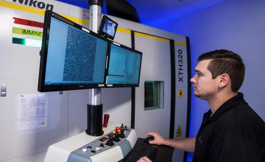
Metal powder for additive manufacturing being inspected using Nikon Metrology micro CT scanner at Sintavia
Almost every industry has seen explosive growth in additive manufacturing (AM or 3D printing) of metal components, either for prototyping or low to medium volume manufacture of often high value and safety critical parts. The powder bed method of fusing successive layers of fine metal powder using a laser or electron beam is one core technology. Alternative methods include direct metal deposition via a nozzle, the latter technique sometimes being combined with subtractive milling and drilling in a machining center. In some systems, dissimilar metals can be combined in the same build cycle to create specific thermal or electrical properties.
The great advantage of AM is that it can produce parts with internal features that are impossible to manufacture by conventional methods, such as curved, conformal cooling channels close to the surface of a mold. AM is also chosen where weight needs to be saved, such as in aerospace and medical component production. Using a touch probe, the resulting filigree structures hidden inside are difficult to inspect without damaging them, therefore call for noncontact methods.
In any case, non-contacting methods are superior for assessing the true geometry and appearance of a surface.
As far as inspecting such features is concerned, internal channels are invisible from the outside so not within the scope of conventional metrology, while fine features and thin walls, although they may be visible, can contain small inclusions that are difficult to detect. The problem with AM parts is that, unlike with most machined or cast components, even very small defects can grow and lead to cracking and catastrophic failure.
For quality assurance of these products, in order not only to reject faulty items but also to allow the AM process to be optimized, the technique of choice for seeing inside metal structures is industrial X-ray computed tomography (CT). For this, an object is rotated through 360 degrees so it can be imaged from all directions hundreds or even thousands of times using penetrating radiation. The rotation may be start-stop or continuous, circular or helical. Using the most powerful equipment on the market, scan times can be as little as a few tens of seconds but typically range from five minutes up to an hour.
A computer algorithm reconstructs the object’s internal 3D structure from the intensity values in the projected images by calculating the X-ray linear attenuation coefficients, which can be interpreted as material density, at all points within the 3D volume containing the sample. However, for this to work well when the structures being tested are metallic, the equipment must be of high enough energy to penetrate the dense materials and produce usable results for analysis.
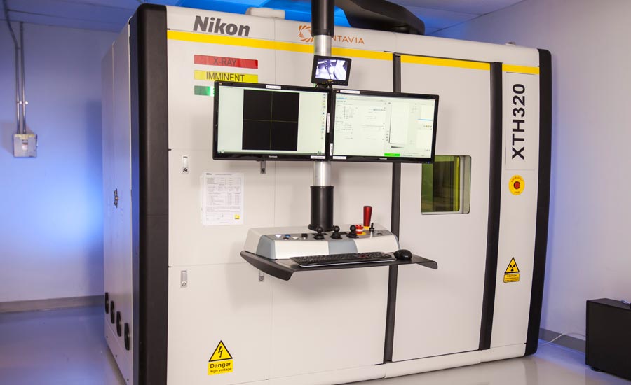
Nikon Metrology’s XT H 450 scanner is often selected for the job owing to its 450kV micro-focus X-ray source. The target is liquid-cooled to allow a high flux to be used, while a flat panel detector is built in to speed non-metrology inspection. The manufacturer has developed a proprietary curved linear diode array target that optimizes X-ray collection without capturing undesired scattered rays, resulting in sharp, high contrast images.
The X-ray tube has a small spot size of between 50 and 113 microns, which delivers a scatter-free CT volume with 25-micron measurement repeatability and accuracy as well as allowing greater magnification for detecting and measuring the minutest of defects. That is because the smaller the spot size, the lower the geometric unsharpness in the image, which is the loss of definition that occurs because the X-rays do not originate from a single point but rather over an area.
The advantage of CT technology is that not only can the presence and position of defects such as voids, porosity, unfused powder and inclusions inside an additively manufactured structure be seen, but it is also possible to nondestructively and accurately measure them and other features, such as internal geometries and undercuts. CT equipment can provide a 3D density map of the internal structure, extract surfaces, create surface and volume meshes and even run simulations of, for example, stress/strain or heat/fluid flow. The most complex free-form surfaces can be captured and compared with the CAD model using color-coded graphics to show compliance.
Additionally, CT allows the source powder to be evaluated before AM even starts, minimizing the risk of defects occurring in the first place. Individual grains of powder in a few slices taken through a small amount of powder are checked for voids, which can cause the grains to explode when heated, blowing away neighboring grains and leaving a hole in the product.

CT analysis of additive manufactured part showing void analysis along with internal / external dimensional inspection, CAD comparison with color map, and sectioning of CT image.
Process Control In Additive Manufacturing
To gain an insight into how the technology works in practice, take Florida metal additive manufacturer Sintavia. It has installed a 450 kV micro-CT scanner to help control the manufacturing processes in its eight powder bed machines, which employ either laser or electron beam melting. In this way, it maintains the highest standards of quality for its clients in the aerospace and defense sectors. Components are currently manufactured mainly from nickel, aluminum, titanium, and stainless steel alloys.
Brian Neff, Sintavia’s CEO, said, “We are making it a mission to work with our customers to develop optimal parameters for their builds. If you don’t understand and control the process, you won’t be able to build what you want to. This demands nothing less than total process knowledge and understanding and full control over the quality function, which is why we decided to install CT scanning in-house rather than outsource it.”
He added that manufacturing standards are highest in aviation, driving the need for a process that is robust and repeatable to raise and confirm component quality. It is essential to understand whether parts are completely free of residual powder after a build, prior to furnacing. It is also necessary to know whether the dimensions of the part conform to those of the design.
By converting 2D pixels to 3D voxels to generate a full 3D density map of the samples, the technique gives all this information in a visual, easy-to-interpret format and shows any departure from the CAD model. It is straightforward to detect and measure powder residues blocking channels, porosity, contamination, cracking, warping, and dimensions such as wall thickness to an accuracy within tens of microns. Given a 100 mm sample and a detector 2,000 pixels across, the limiting resolution is 50 microns, and, by interpolation, measurement accuracy is up to ten times better than this.
CT analysis of additive manufactured part showing void analysis along with internal / external dimensional inspection, CAD comparison with color map, and sectioning of CT image.
Conclusion
Provided that the X-ray equipment used is of sufficiently high resolution to detect and measure features and flaws down to tens of microns in size, it is ideal for carrying out exhaustive, nondestructive quality control of additively manufactured components up to 300 mm across.
It is able to inspect source powder for voids and inclusions, check for correctly printed structures, compare the part against the CAD model, find and measure defects in parts, identify entrapped or unfused powder and perform dimensional analyses. It therefore supports faster optimization of AM prototyping and production processes. Historical records can be kept in digital form for traceability and future interrogation should there be queries regarding quality after the part has been in service. NDT
Looking for a reprint of this article?
From high-res PDFs to custom plaques, order your copy today!


