X-ray Increases Product Quality
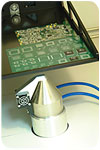
Impressive image resolution and magnification enable operators to clearly visualize flaws in electronic substrates. Source: Nikon Metrology
Quality control at Mentzer Electronics (Burlingame, CA) includes tracing electronics assembly issues using Nikon Metrology’s (Brighton, MI) Metris XT V. This electronics X-ray inspection system allows quality engineers to navigate through the internal structure of assembled printed circuit boards (PCBs). In the rapidly evolving electronics industry, Mentzer Electronics uses the acquired insight to improve manufacturing processes.
Subtle defects such as metallic dendrites, voids and improper solder flow may not cause instant system breakdown during electronic testing. X-ray inspection is no luxury; it is necessary to verify electronic connections, which are mostly invisible from the outside. Mentzer started X-ray inspection with a tabletop system that soon showed limitations in terms of image quality and specimen size.
“Three years ago, we opted for a dedicated electronics X-ray system from Metris, which outperforms the tabletop system in every performance aspect,” says Ed Mentzer, founder and chief executive officer of Mentzer Electronics. “Metris XT V helped us trace tricky defects that we would otherwise never have found.”
Verification, Troubleshooting and Repair
“Mentzer and Metris has been a good marriage,” says Mentzer. “We use the micro-focus X-ray system for quality verification, troubleshooting and repair of PCBs, cable connectors and wire harnesses. Using real-time X-ray, we intuitively navigate inside a PCB and zoom in on anything suspicious that catches our attention. Impressive image resolution and magnification enable us to clearly visualize a wire bond flaw in integrated electronic circuits, or trace incomplete vertical interconnect access causing electronic disconnection between PCB layers. By tilting the PCB manipulator tray, we obtain angled viewpoints that make it easier to investigate ball grid array (BGA) connectivity, multi-layer boards and solder joints.”Over the years, Mentzer Electronics gradually extended its in-house production capability in order to deal with larger and more complex electronics manufacturing services. Today, the company’s electronics engineering laboratory is equipped with component place machines, soldering machines, in-line cleaners, surface mount reflow ovens, lead-forming machines, wire cut and strip machine and PCB stencil printers.
Mentzer mentions that his assembly engineers use the Metris XT V system to trace problems, analyze them and define the most appropriate countermeasures. Concerning a PCB batch that they recently manufactured to go into scientific instruments, X-ray revealed an internal bridge. After detailed analysis, they decided to resolve the bridge by applying a very fine drill cut into the board and manually removing the bridge. As it turned out to be a repetitive manufacturing error, this countermeasure was copied on all PCBs of the batch. “This successful intervention saved us many thousands of dollars on material cost and staff expenses, and secured timely product delivery to the customer,” says Mentzer.
According to Mentzer, BGA inspection was the original aim of the X-ray system purchase. He explains that angled views really help quickly and confidently spot connectivity issues caused by smaller or irregular BGA balls.
Tight regulation
Electronic PCBs, racks and cabling are built into end products that serve different purposes. For a medical firm, Mentzer manufactured control electronics for a spine surgeon table. Engineers performed X-ray quality verification at different stages in PCB manufacturing and assembly and also monitored wiring harness production. A new tendency at Mentzer is that it receives more and more services orders from firms involved in ecologic projects, including solar and wind power generation. Activities for such projects include electronics manufacturing of charging batteries for solar controllers and electronic controls for wind turbines.Mentzer also takes systematic action regarding compliancy with ever-tighter regulations. One example is the use of lead-free solder material, which is imposed by European Union hazard regulation. “The use of lead-free solder sets specific challenges, as this type of solder flows quite differently than regular thin lead solder,” explains Mentzer. “Solder-related lessons learned through X-ray enable us to optimize the operation of our soldering machines and surface mount reflow ovens. Although many processing steps are automated, the quality of the end product often depends on details that need to be just right.”
Improved Practices
“The bottom line is that with Metris XT V, we are able to quickly trace internal errors that otherwise remain hidden in the product,” summarizes Mentzer. “This immediately impacts product quality, and indirectly, we use the acquired insight to further improve and speed up our manufacturing practices. Key is this strategy is that the system is self explanatory and provides high image quality and sharpness. Maintenance is low in cost because the system contains an open-tube source, which allows us to quickly exchange the filament ourselves. Another advantage is that we can easily shift the small-footprint machine to another location in our facility without having to worry about a high-voltage power connection or special floor conditions.”Nikon Metrology Inc.
(810) 220-4360
www.nikonmetrology.com
Benefits
Looking for a reprint of this article?
From high-res PDFs to custom plaques, order your copy today!


