Looking Internally with Computed Tomography
Users from electronics manufactures to paleontologists see benefit of nondestructive inspections.
Industrial inspection equipment doesn’t appear in mainstream news on a regular basis. But that’s what happened when Samsung found itself in the unenviable position of determining why its Note 7 smart phones had turned pyrotechnic.
Within weeks of its 2016 debut, customer reports emerged of the phone catching fire—or even exploding. The disaster cost the business a quick $26 billion in the stock market, according to the Washington Post. A series of recalls followed, again costing the company billions.
Samsung eventually used computed tomography to determine fatal flaws in the lithium-ion batteries, using the industrial X-ray equipment to find internal problems. It was eventually determined that batteries from two different suppliers were faulty. One didn’t leave enough room between the positive and negative electrodes in the battery, which caused “electrodes inside each battery to crimp, weaken the separator between the electrodes, and cause short circuiting,” according to an article in Wired. Problem batteries from the second supplier missed insulation tape, and some contained “sharp protrusions inside the cell that led to damage to the separator between the anode and cathode. The batteries also had thin separators in general, which increased the risks of separator damage and short circuiting,” according to Wired.
Computed tomography played a key role in finding the defects after they already became a problem. Clearly, quality control is more beneficial before the international rollout of a faulty product, and computed tomography is increasingly being used for inspection across the electronics, aerospace and automotive industries, in addition to research projects for one-of-a-kind prototypes and other valuable specimen.
CT scanning “allows you to inspect an object in its internal detail,” explains Justin Gladman, R&D engineer at Duke University’s Shared Materials Instrumentation Facility. “X-rays can obviously pierce through most things of a certain density, and it does that nondestructively, which is the second thing we like. The examples that I’ve given—people who are bringing in fossils or even devices that we’ve created in our nanofab facility—if you’re spending all this time building a chip or you uncover a one-of-a-kind fossil, you both want to know what’s inside of it and what’s this micro level detail that I’m looking at. You also want to know that without destroying a one-of-a-kind object.”
The Shared Materials Instrumentation Facility (SMiF) is part of Duke’s Pratt School of Engineering. It provides a place for faculty to share lab equipment.
“We basically offer to give them some space for [equipment] and also we have staff that run the equipment, keep it up, and train people,” Gladman says. “In exchange, they basically are donating equipment to us and we open it up for users across the university and even outside the university to external universities and industry.”
The lab’s CT scanner shares space with scanning electron microscopes, transmission electron microscopes, and other equipment. Researchers in the university’s nanofab can bring devices, inspect them nondestructively and determine if they are building what they are trying to build.
The fact that the lab’s CT scanner sees use from paleontologists, nanofab researchers and everyone in between speaks to the versatility of the technology.
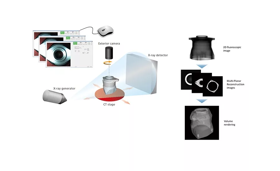
In general terms, a computed tomography scanner has an X-ray source, a detector panel, and a rotary table. The X-ray source takes hundreds or thousands of images of the test specimen as it rotates on the turntable. Computer software then reconstructs the images into a 3D volumetric model containing billions of voxels. Each voxel is a cube with a discrete x-y-z position and density. The model can then be digitally cross-sectioned and otherwise inspected for a range of analyses including voids, inclusions and other defects. Computed tomography scanners today can also make metrology-grade measurements of both internal and external features. Other popular modes of use include wall thickness analysis and carbon fiber composite material analysis, where software can analyze the direction and orientation of embedded carbon fibers.
Micro-focus non-destructive X-ray testing and inspection systems are widely used in many areas of research and development for morphological and structure alternation analyses, and for quality control purposes related to preproduction inspection, failure analysis, and lot inspection, according to information from Shimadzu.
The technology has also grown along with the increased use of additive manufacturing. 3D-printed parts have internal geometries more complex than previously possible with traditional, subtractive manufacturing, and computed tomography allows technicians to inspect those features without altering their composition.
As electronics become smaller and more internally complex, manufacturers can learn a valuable lesson from Samsung and nondestructively inspect parts before they self-destruct.
Looking for a reprint of this article?
From high-res PDFs to custom plaques, order your copy today!


