Measurement
Metrology and Microscopy for Electronics Quality Assurance — in One Machine?
Compliance can often only be achieved through both metrology and microscopy tools.
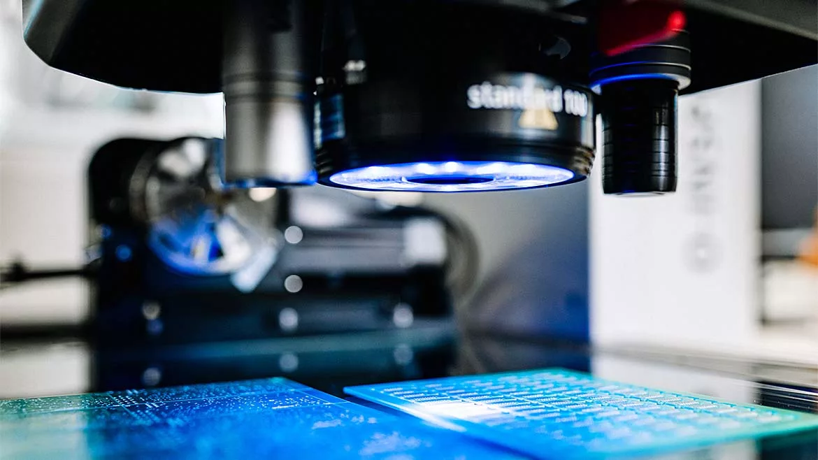
Printed circuit boards (PCBs), printed circuit assemblies (PCAs) and batteries, in particular, need advanced metrology and inspection equipment to build high reliability components that are important for New Energy Vehicle (NEV), aerospace and spacecraft, and medical device creation. Source: ZEISS
Electronics parts, components and devices can be complex, requiring meticulous manufacturing processes to ensure the performance of the finished product.
Printed circuit boards (PCBs), printed circuit assemblies (PCAs) and batteries, in particular, need advanced metrology and inspection equipment to build high reliability components that are important for New Energy Vehicle (NEV), aerospace and spacecraft, and medical device creation. The growing demand for miniaturization and high-density interconnects make it increasingly difficult to identify defects, meaning a need for inspection systems that can do traditional metrology applications and optical inspection tasks in microscopy.
The good news is that technology is on the horizon for electronics manufacturers. Both metrology and microscopy technologies will combine to fulfill high-end Geometric Dimensioning & Tolerancing (GD&T) tasks, along with image analysis techniques required for new product development and failure analysis inspection.
What are the market demands and expectations for electronics?
A lot of it has to do with the standards used by the electronics manufacturing industry and new trends. All safety and function-critical components must comply with class 3 IPC standards, evolve with industry trends, and meet sophisticated customer expectations. This compliance can often only be achieved through both metrology and microscopy tools.
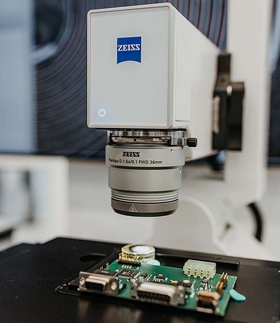
Many electronics manufacturing applications require microscopy tools for visualizing and segmenting parts. These applications include:
- GD&T dimensional measurement
- Visual inspection for failure analysis
- Process control of existing products
- New product development prototype inspection
- Solder joint dimensional verification
- Visual inspection of defects, solder balls, trace bridging and voids for example
- Micro section analysis of multi-layered structures
- Optical measurement
- Surface material characterization
These applications are vital for safety-related devices that require measurement and microscopy inspection, such as:
Electronics
- High reliability PCA products for aerospace, military, industrial IoT and medical devices
- Battery foils which are cut or punched out of coated copper, and aluminum or insulation paper foils which need to be examined for shape and particle contamination
- Display panels in electronic products utilize sensitive and difficult-to-analyze materials that require microscopy technologies for defect detection and geometric verification
NEV
- Fuel cells have individual stacks that require the highest quality standards in production and development of each individual component
- Battery foils that undergo chemical and structural changes due to frequent charging and discharging
Medical Devices
- Class 3 medical device implantable electronic assemblies that can’t fail
Overcoming bottlenecks in the quality lab
Requiring both metrology and microscopy equipment for your quality assurance program may be causing bottlenecks in an overcrowded lab:
- Lengthy setup time on multiple machines for a single product
- Colleagues may struggle with identifying efficient workflows and processes
- Metrology equipment might block microscopy machines, or metrologists will interrupt microscopists for support in inspecting defects on a workpiece
- Microscopy equipment stage size limitations; many are not large enough for today’s PCA and battery assemblies
- Large products can be problematic for electronics manufacturers who want to perform nondestructive inspections. Destroying components for measuring and inspection due to their size takes time as does multiplying sources of errors by cutting workpieces and moving between different systems
While Class-2 parts are highly reliable but can be fixed if needed, Class-3 parts can’t fail in aerospace and space. PCBs and PCAs are Class-3 parts that must undergo GD&T and inspection at a fine level.
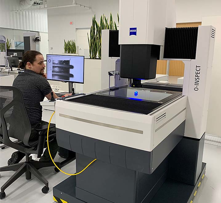
One tool, two functionalities
Unfortunately, most coordinate measuring machines (CMMs) do not have typical microscopy functionalities and most microscopes do not have typical metrology tools. In addition, many industrial metrology manufacturers have systems with color cameras but not microscopy tools.
The ideal would be a synergy of both machine types. The result would have many compelling benefits, such as:
- Large stage capabilities, allowing measuring and inspection for workpieces up to 800 x 600 x 300 mm
- More cost-effective than buying two machines
- Two dedicated software packages, for measurement and inspection, working in tandem to handle every quality task
- Improved internal workflows and saves time and resources
- Metrology with color images
A paradigm shift in quality assurance
Electronics manufacturing utilizes both metrology and microscopy technologies to perform quality assurance, but they are not optimized in their current form. Soon, we expect a paradigm shift for industrial metrologists, quality laboratories and measuring laboratories.
The first-to-market technology will have an impressive array of features, including:
- Combined 3D measurement technologies and microscopic inspection in one machine for better integration and efficiency.
- A large inspection field for microscopy
- Combination of functionalities with the advantages of two machines offers sustainable and cost-efficient solution
- An integrated software package, scalable to both metrology and microscopy needs
One combined software package from both worlds brings a lot of power to one machine. The universal measuring software enables automated metrology, imaging and documentation of large components or for multiple parts at high throughout. The microscopy software facilitates HDR image acquisition, panorama and tiles, autofocus, enhanced depth of field, layer thickness measurements, technical cleanliness analysis, inclusion analysis and comparative diagrams.
Perhaps the most impressive functionality of the microscopy software is image segmentation with machine learning (ML). Automated segmentation can be reliable but not always exact, as patterns in images evident to the human eye may not be identifiable by a computer — or the other way around. ML, however, can combine human and computer insight to amplify image segmentation possibilities and produce more precise segmentation data.
Accelerating toward the future of quality assurance
What's on the horizon for electronics manufacturers? Good things, with solutions to optimize inspection processes and minimize quality lab footprints. Soon there will be fast, flexible, and precise systems and software that combine CMM technology and microscopy inspection into one unique solution. Yes, one machine.
Looking for a reprint of this article?
From high-res PDFs to custom plaques, order your copy today!


 machine.")

