Quality Measurement: Extending the Frontiers of Noncontact Surface Inspection
Development of noncontact optical inspection solutions often can provide a level of product quality assurance that is not affordably achievable by either human visual inspection or by general-purpose inspection products.
The pace of progress in precision manufacturing in all industry sectors is creating an ever-increasing demand for new and innovative methods for noncontact inspection of manufactured part and assembly surfaces.
Sometimes existing products can be found to perform the required function in terms of resolution, speed, robustness, field-of-measurement, depth-of-measurement, sensitivity and the many other factors that define an application’s requirements.
But more often, the desired higher level of manufactured item quality and performance requires the development of new solutions that stretch the state of measurement and inspection technology in one or more critical directions. Often three-dimensional (3-D) inspection is a critical part of the solution.
In most industrial and commercial sectors, the benefits of automated noncontact surface inspection are clear and substantial. They include most or all of the following factors:
The technologies of lasers, optics, dynamically controlled illumination, photonic sensing, image and signal processing (or vision) algorithms and software, and even mechanical part and surface positioning all come together as multidimensional ingredients of each advanced noncontact surface inspection solution.
All of these technologies are advancing steadily albeit at different paces. What was not possible last year and last month is now often readily achievable with expert system engineering and integration. Technical solutions offered to satisfy proven large markets are often not as capable as can be provided to meet a specific focused application’s requirements.
Solution Requirements Definition
The starting point of an advanced application solution is the careful, knowledgeable and quantitative definition of the complete set of application requirements. This involves much more than simply stating what must be detected or measured and how rapidly the solution must operate. As Albert Einstein famously said: “Things should be kept as simple as possible, but no simpler.”Surface inspection inherently entails detecting and often measuring surface phenomena-some considered to be defects and others considered to be just acceptable artifacts or desired features. These have some range of sizes, visibilities, optical spectral, scattering, polarization and other characteristics. The surfaces themselves also have important characteristics-perhaps consistent and perhaps highly variable in space or time.
An application’s end-user and the solution development engineering team must work together to identify all parameters and trade-offs that will define the bounds of acceptable and optimum solutions for the application.
A few of the usual questions include:
Agreement on clear and quantitative answers to questions such as these is a key starting point for ensuring that all expectations are aligned and a responsive development can be proposed and executed.
Exploiting the Pace of Technology Progress
A substantial range of technologies is available, each best suited to a subset of inspection applications defined by those answers. With today’s newest technologies, an advanced surface inspection solution can replace tedious, distracting and fatiguing manual tasks, detect defects not visible to a human operator, process surface areas faster than human visual perception can accomplish and perform detection, as well as the measurements that often are critical in judging defect severity.Recent underlying technology breakthroughs of particular value include:
Along with advances such as these, the availability of ever-increasing low-cost computer power and the extended performance and reliability of light sources ranging from lasers to LEDs allow reliable systems to be devised for continuous operation on plant floors or elsewhere.

Successful Development Strategies
The most prudent approach to accomplishing an advanced solution development is a step-by-step experimental and analytical series of planned project phases. These typically consist of:An experimental and analytical feasibility investigation phase. This is designed to “home in” on the best overall approach to meeting the original requirements that were as defined as described above. The result will be a report of feasibility findings and a description of the proposed system concept. This phase may require weeks to a few months.
The engineering prototype phase. In this phase, a working implementation is created to demonstrate the fundamental capability that is required. At this stage, system packaging and peripheral features or functions may be deferred in the interest of achieving an economical “proof of principle.” Examples of deferred features might include speed or operator convenience functions. This phase may take from several months to as long as a year.
A fielded prototype (if quantities of systems will ultimately be desired) or a final system delivery phase. In this phase, a complete packaged system solution will typically be built, tested, validated and installed either in an evaluation setting or in the final end-use venue. This phase may require several months to as long as a year for completion depending on the operating and environmental requirements for the ultimate system.
If the desired solution will be desired in substantial quantity, then the fielded prototype phase may be followed by a manufacturing engineering phase aimed at cost minimization, producibility engineering, reliability engineering or other objectives. The result will normally be a production prototype. Several months will usually suffice for completing this phase.
The manufacturer today who seeks to supply products with high perceived and actual quality at competitive costs must seriously examine how his product’s external and internal surfaces and appearance will be reliably and 100% inspected at high resolution, while not adversely impacting his production rates and other operating requirements. The specific types of variances and defects to be detected and avoided will differ across product classes.
Development of noncontact optical inspection solutions, focused on a specific product’s characteristics and requirements, often can provide a level of product quality assurance that is not affordably achievable by either human visual inspection or by general-purpose inspection products
Quality Online
For more information on noncontact surface inspection, visit www.qualitymag.com to read the following:Tech Tips
CASE STUDY 1
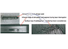
Laser welding is increasing in its importance due to significant energy savings, speed and avoidance of excess metal margins around traditional spot welds. But defective laser welds caused by incomplete material fusion must be avoided. By use of a controlled laser light source and infrared imaging as welds are made, defective incomplete welds can be immediately detected and the location of the defect can be isolated with high resolution without use of tedious and destructive testing procedures. Source: Coherix
‘
CASE STUDY 2
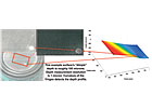
Minor cosmetic or dysfunctional dimensional defects on bare metal surfaces, even those that are too subtle for the human eye and brain to discern, can be detected and measured by rapid interferometric sensing of surface deformations. These defects, if not detected, can become unacceptably more visible when the metal surface is finally finished or is placed in adverse lighting conditions. Or they can even prematurely fail when the part is put into operation. Illustrated is a portion of a surrogate surface. An entire curved or flat surface shape can be measured to a few microns of accuracy in seconds. Source: Coherix
CASE STUDY 3
Microscopic surface corrosion defects at the micron level can affect the strength or function of large critical structural elements. This surface degradation can be detected and measured using multi-wavelength holographic interferometry as shown for a familiar corroded steel artifact. The 3-D extent/depth of detected corrosion is measured to submicron accuracy. Source: Coherix
CASE STUDY 4
Products subject to various specific types of surface contamination can be inspected with computer-controlled multispectral illumination and sensing to discriminate acceptable surface artifacts from contaminants on all surfaces at a rate of tens of thousands of product units per hour. Shown are different contamination types and areas found on 3-D object surfaces on the fly. Source: Source: Coherix
CASE STUDY 5
Products processed at blinding speeds during fabrication, coating or assembly are usually either small in size or very detailed in their required surface characteristics. New-generation sensor and processing technology allows them to be inspected at production rates that a human visual inspector simply cannot match for any useful length of time. Source: Coherix
Looking for a reprint of this article?
From high-res PDFs to custom plaques, order your copy today!


