CT Inspection: An Inside Look at CT-Based Nondestructive Testing
CT scanning has become an important tool for many research, industrial, and safety critical applications.
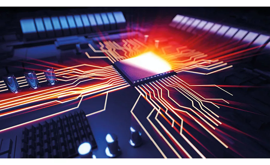
RF Power
What is computed tomography (CT) scanning?
A leading technology in the medical field since the 1970s, CT scanning is now taking its rightful place as a powerful observational tool in the industrial realm. A CT scan is a three-dimensional density map of any object that can be penetrated by the beam. The CT scan is generated from 2D projection images of the part onto a digital detector array (DDA), or from single rows of CT slices from a linear diode array (LDA). Once these images have been reconstructed, CT analysis software allows users to virtually slice the object in any direction, allowing them to measure internal structure and flaws. Adoption of this technology has enabled users to visualize internal structures in ways that previously could only be done by destructive methods. CT scanning has become an important tool for many research, industrial, and safety critical applications where the user needs to “see” inside an object without destroying the object in the process.
Five Things You Should Know before Buying a 3D Industrial Computed Tomography System
1) Application Insight: When would you use CT scanning?
CT scanning is utilized by a very diverse group of users. From university researchers to museums, factories and government labs, there are many applications where a user needs to observe the internal structure of an object.
Industrial applications are typically specified in terms of cycle time required, along with a definition of acceptable image quality, defect types, and sizes. These are usually specified by the manufacturer. If the industrial user plans to use the equipment for different objects, it helps to identify all of the various applications to ensure the system selected can perform the required inspection tasks equally well.
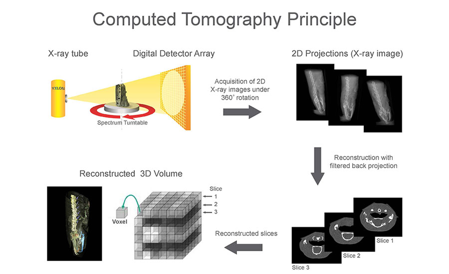
Computed Tomography Principle
Successful CT techniques have been developed for materials analysis, defect recognition, failure analysis, statistical process control, metrology, assembly analysis, image-based finite element analysis (FEA), and reverse engineering. Reverse engineering is a way to “recreate” a legacy physical component, which may not have an applicable engineering drawing. Performing a CT scan on a legacy object is often the first step in creating engineering files needed to rebuild them with additive manufacturing (3D printing) or other methods. CT is also used to provide feedback for “dialing in” production parameters for additive manufacturing methods by making it possible to see internal problems such as voids, entrapped powder, lack of fusion, inclusions, and powder contamination.
X-ray and CT
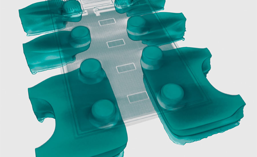
Today, many parts may be designed in one country, machined in a second, and assembled in a third. Verifying that the part matches the original CAD design is critical, especially if the part is to be used in an assembly. Industrial CT allows users to compare parts to one another or to CAD data. The deviations of external and internal geometries can be shown on a surface color map chromatically on the 3D representation or by whisker plots in 2D slice windows. This process is useful to compare the dimensions of parts sourced from different suppliers or manufacturing processes, such as studying the differences in parts from one cavity to another cavity from the same mold. The “nominal/actual comparison” is also useful when comparing parts subject to different loading or environmental conditions.
ebeam
2) Based on the available technical capabilities, which system can best meet your application requirements?
You can make better buying decisions when you’re aware of the different kinds of advanced technical options available to you. Many industrial CT systems on the market today, no matter the manufacturer, use the same third party analysis software. The key differences can be evaluated by having your parts scanned by the different vendors, comparing image quality, and evaluating the ergonomics and ease of use of the systems in person. Once you have evaluated these factors and selected a solution, the vendor will work with your system operators to fully optimize the techniques used for your application.
Example of nominal vs actual, courtesy of Volume Graphics Studiomax. (www.volumegraphics.com/en/products/vgstudio-max.html)
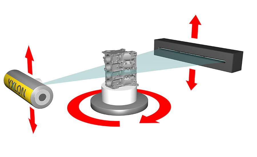
Another alternative is helical CT. This form of CT scanning generates a single, seamless 3D dataset for long objects. It can create better quality images in situations where a normal cone beam CT would generate stitching artifacts, or poor image quality at wide cone-beam angles. Helical CT works by simultaneously rotating and translating the object being scanned, eliminating the need for image stitching.
Helical CT
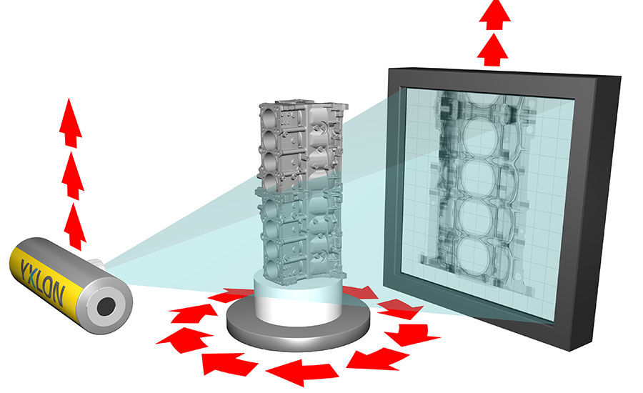
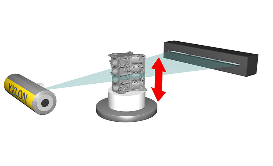
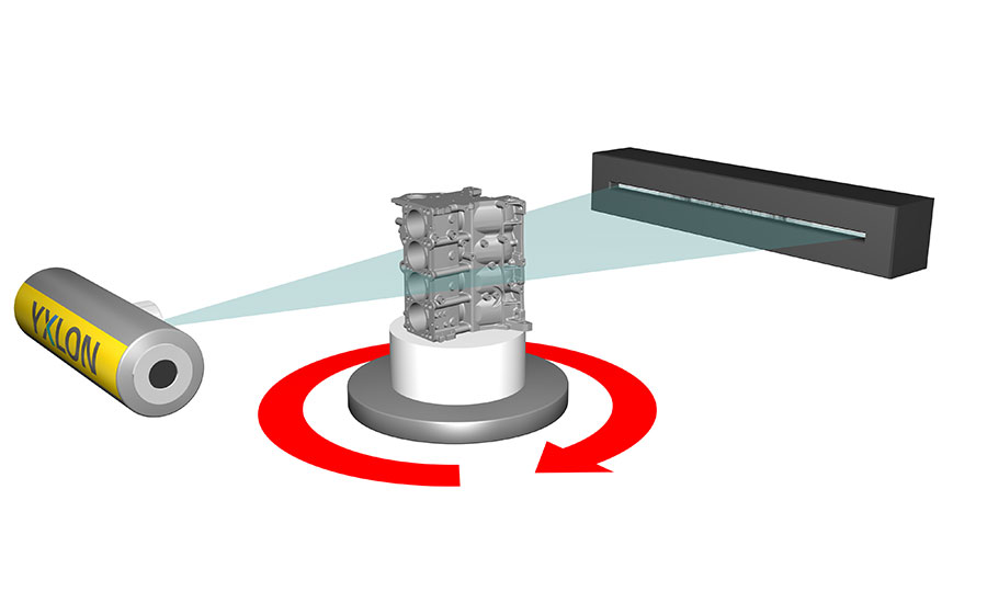
Traditional fan beam CT data is generated by a fan-shaped X-ray beam that is captured by a linear detector array (LDA). Producing a 3D CT data set from a fan beam system involves rotation of the scanned object followed by vertical movement of either the object or the tube and detector. This sequence is repeated until the target area is scanned. Fan beam CT systems are ideal for scanning single slices, for large and dense parts which normally require higher X-ray energies (≥ 320 kV).
With cone beam CT, a flat panel (DDA) sensor captures a cone-shaped X-ray beam. Cone beam CT systems are ideal for polymers, small metal castings, medical devices, biological objects, additive components, electronic components, and generally any object that fits in a 32” cube with density of aluminum or less. If the application requires producing a full 3D model and the image quality is sufficient, cone beam is often the best choice. For one thing, it allows you to acquire a typical data set in 15 minutes or less. However, if the object is larger than that, or more dense than aluminum, then a few slices with an LDA can often produce better images faster.
3) Paying more for convenience can save you more in time.
Buying the lowest cost system might end up costing you more in the end. For example, the manipulator that moves the object to be scanned must be precise if you want to obtain high quality measurements. Purchasing a system with a lower quality manipulator can lead to lost time and extra cost.
Fan Beam Scan
If a CT system is going to be used for measurement purposes (metrology), first evaluate that system to see if it meets your requirements for accuracy and repeatability. Some vendors’ CT scanning process may involve a calibration step prior to each scan, and some do not. This may affect the overall cycle time. Also every vendor typically has a different way to validate their measurement accuracy with an artifact. An interested customer should not only evaluate this process but also conduct applications studies on their own samples. Measuring an artifact is never the same as measuring an actual part, especially when one considers different shapes and material densities which can all contribute to artifacts in CT imaging. These artifacts can affect the measurability of a feature. CT is a great tool but cannot always solve every manufacturing or measurement requirement.
4) If one CT system can’t cover 100% of your applications, consider a vendor with additional scan services.
Delegating to an expert can be a wise strategy. Consider this: what happens when you realize that your CT system is not equipped to handle all of your applications? When you need to work on a project that is beyond your system’s capability, you may want to consider using a CT service provider to help add what you don’t have. Many vendors provide this service for their customers at a low cost, and even allow trained customers access to their facilities, to run their own parts.
5) Claims about “ease of use” can be deceiving.
Usually, when describing a CT system, “ease of use” refers to the “user friendliness” of the software—but pay close attention to the user interface when the vendor demonstrates how to use it. You may find it is anything but easy compared to another vendor’s software. When making such a big investment, you’re going to want your system operators to feel comfortable with the software.
Another important consideration is how the software relates to the hardware. If calibration scans are required, the process may involve tedious extra steps and cumbersome physical manipulation of the equipment.
Blending Three Product Solutions—How These Technologies Can Be Used Together to Improve Advanced Materials and Processes
Cone Beam CT
Combining the strengths of three powerful technologies creates a synergy that’s hard to beat in the modern manufacturing realm. Working together, plasma control, electron beam, and X-ray and CT inspection technologies can streamline part production like never before for semiconductor and other products.
At a high level, plasma control technologies uses radio frequencies for controlling plasma processes; X-ray and CT are used for nondestructive testing and inspection; and electron beam technology is used for eco-friendly, noncontact treatment of surfaces.
- Plasma control enables inspection to be done on an atomic scale as devices shrink for memory and logic. RF plasma can be used to perform deposition and etch steps at the chip scale level in semiconductor production.
- Electron beam applies very high and low energy plasmas in new and innovative ways. It is used to make composite materials, to alter materials such as in ways that make them more corrosion resistant, and to irradiate food to kill pathogens.
- X-ray and CT imaging inspect inside parts and components for defects, bonding failures in material layers, and quality issues.
- So with all three, companies can construct a complete technology platform—to perform deposition and etch on semiconductors, to change material compositions and to inspect. For instance, an aerospace manufacturer would:
- Deploy RF plasma for industrial coatings
- Use electron beams to change the coatings materials on the blades to make them more corrosion resistant
- Use CT technology to inspect engine turbine blades for defects, bonding thickness or uniformity of coatings, or fatigue analysis
Or, an electronics manufacturer would first perform etch and deposition tasks at the chip level with plasma control, then improve the quality of the chip’s surface with electron beam, and finally test the chip for bonding and defects with CT scanning.
From the microscopic details of a single part to the global vision that focuses on making the most of your applications, CT inspection offers spectacular views.
Looking for a reprint of this article?
From high-res PDFs to custom plaques, order your copy today!


