Analyzing Unexpected Structural Defects in Electronic Components
Anomalies may lie outside the scope of the established imaging parameters.
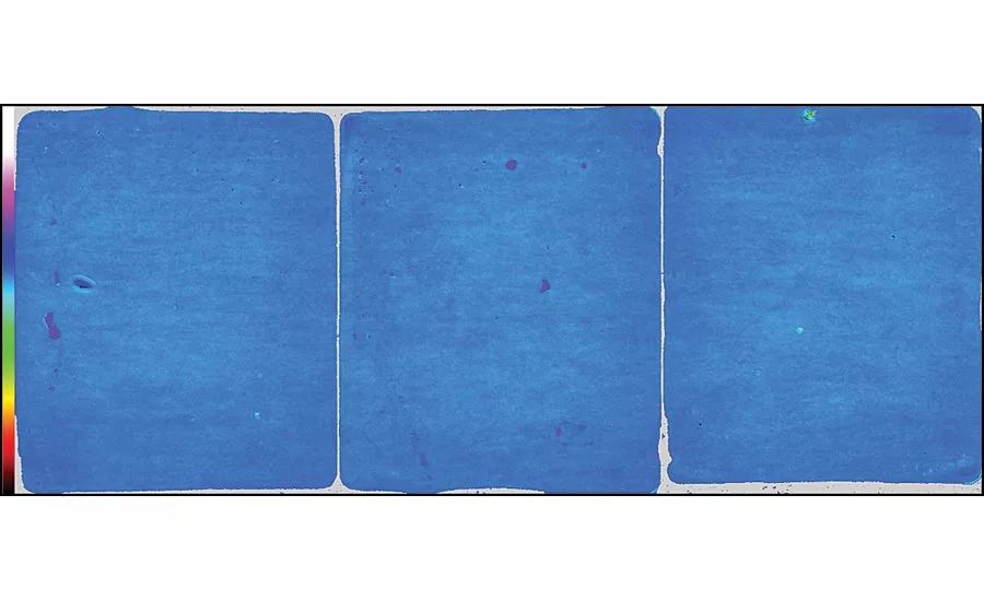
Figure 1. C-mode image in which blue indicates good bonding of solder to the ceramic layer in an IGBT module.
An electronic component on its way to being installed in a system has, it is hoped, no cracks, voids or other internal structural defects that may cause an electrical failure in service. Generally, internal structural anomalies are visible to ultrasound, and a trusted method for identifying components likely to fail is acoustic micro imaging—a tool that uses high-frequency ultrasound for imaging. Laboratory versions of these tools typically examine small numbers of components, but high-throughput automated systems can handle thousands of components, usually carried in trays.
The high-throughput imaging may be performed by the maker of the component, or by the user of the component. In both cases the detailed imaging parameters for trays of a given component are well established and succeed in removing those components that do not meet the manufacturer’s acceptance criteria and that are likely to fail in service.
On occasion, however, anomalies may lie outside the scope of the established imaging parameters. One example: a silicon integrated circuit chip in an epoxy package may be tilted, putting stress on wires and causing other risks. Automated imaging chiefly looks for large voids and other gaps. An automated system has the ability to measure tilt and warpage, but tilt and warpage are not typically included in the imaging parameters.
Tilts and other unexpected failures may become evident in testing, during assembly, or in service. When such things happen, a suitable sampling of the components in question is moved to a laboratory for more detailed acoustic analysis. Most high-throughput acoustic analysis uses what is known generically as C-mode imaging to collect echoes from a specific depth or interface below the surface. This mode is versatile and fast. But there are over a dozen other acoustic micro imaging modes some of which may be less suitable for high-throughput screening but are capable of detecting subtle phenomena. A lab will employ some of these modes to quickly and accurately diagnose a problem.
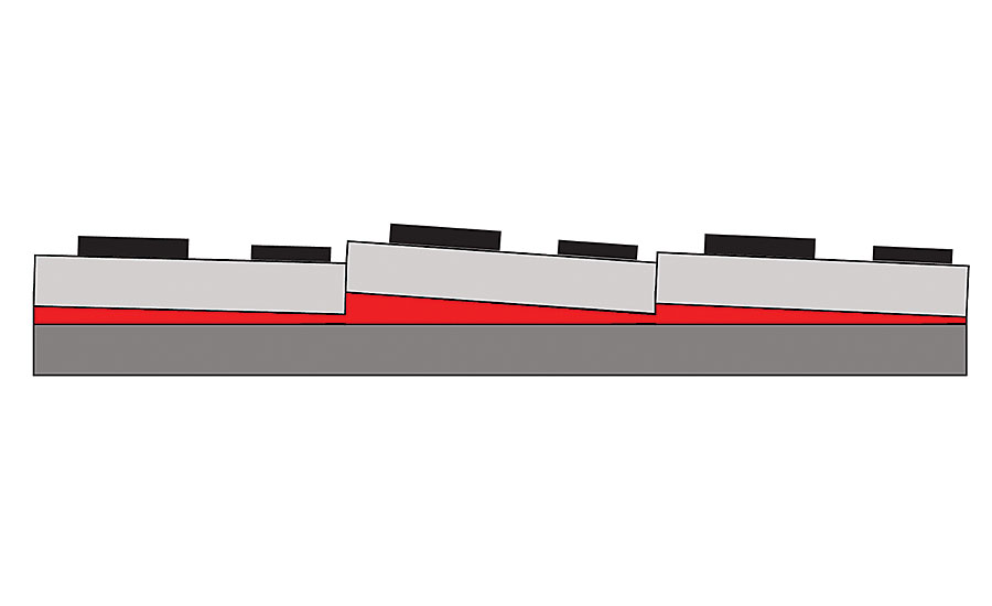
Figure 2. Diagram of an IGBT module where the bonding is successful but not horizontal.
In C-mode imaging, the transducer scans just above the surface of a component, and the ultrasound is coupled to the surface by an accompanying water jet. Dozens of times per millisecond it launches focused ultrasound pulses into the component and receives echoes from interfaces between materials. The bond between two solids sends back some of the pulse’s energy as an echo. The rest crosses the interface and travels deeper. Where a solid meets an air gap, 99+ percent of the pulse is reflected, and none crosses the interface. When an echo arrives at the receiver, its amplitude and phase are measured to learn about the interface from which it was reflected. C-mode can thus image voids, delaminations, cracks, non-bonds and the like, in addition to characterizing the bond quality between solid features.
The failure analyst trying to track down the root cause of an unexpected failure may use C-mode imaging to gain an initial overview of problem parts, and then move to more specialized acoustic micro imaging modes. Three of the more specialized modes are discussed here.
The Time of Flight and Time Difference (TD) Modes
Ultrasound travels through a material at a specified speed, measured in meters per second. Through mold compound or plastic encapsulant, for example, ultrasound travels at about 3,000 meters per second. When a pulse leaves the transducer, the first material interface it encounters is that between the water coupling and the surface of the part. This echo is not generally used for imaging, but rather as a starting point for measuring the time it takes for a pulse to cross the surface, reach a material interface, and return to the surface and the transducer. This imaging mode, which is called Time of Flight (TOF) measures time in nanoseconds and is used to measure the depth of an interface from the surface of the part.
Because the transducer collects thousands or millions of echoes in scanning a single part, the depth of an internal interface can be determined wherever an echo was received. Whereas C-mode imaging uses the amplitude of an echo to image the interface, TOF uses the travel time of an echo to determine the depth of the interface at a given x-y location.
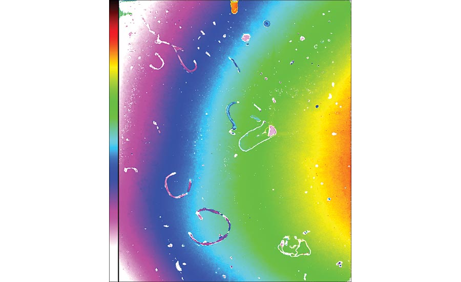
Figure 3. Time Difference mode reveals tilted die and nonuniform thickness of solder in the center substrate in Figure 1.
The Time Difference Mode (TD) measures the thickness of an internal material layer by measuring the separation in travel times between two adjacent echoes. This measurement is turned into a color indicating the thickness of the layer at each x-y location. In this way color is used to create what amounts to a map of thickness variations of an internal layer.
Figure 1 is the C-mode image of an IGBT (Insulated Gate Bipolar Transistor) module having three ceramic rafts. C-mode was used to determine whether, and how well, the solder was bonded to the ceramic layer below it. The amplitude of each returning echo was measured and assigned a color. The resulting image of the whole module uses only a tiny part of the range of colors available in the color map at the left margin of the image. Conclusion from C-mode imaging: virtually the total area between the solder and the ceramic is well bonded. There are no significant voids or delaminations between the solder and the ceramic, and the likelihood of a field failure from such defects is tiny. But higher magnification of this sample revealed small voids and other small anomalies.
One of the problems found in IGBT modules is that the solder layer may not have a uniform thickness in all areas. Instead, a cross section of the module might look something like the exaggerated diagram in Figure 2. Red marks the solder; the base plate is below the solder; the ceramic and die are above the solder. There may be no voids in the bulk of the solder, but what matters in this situation is the variable thickness of the solder, which will create different rates of heat dissipation in different regions of the die. Stresses resulting from these thermal variations can cause the die above the ceramic to fail.
Figure 3 is the Time Difference image of the center component in Figure 1. Figure 1 reveals that the bond between the solder and the ceramic has few if any significant disbonds, but Figure 3 reveals that the bond between the solder and the ceramic is tilted and warped in two dimensions. The thickest regions are white, while the thinnest regions are red. The numerous scattered features are voids in the solder.
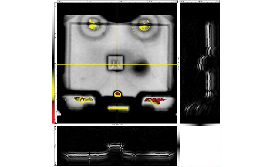
Figure 4. The virtual rescanning module created these images from the matrix file of a physically absent TO-247 power device.
Virtual Rescanning Module (VRM)
After a component has failed in testing or in service, it would be useful to go back in time and acoustically image that component in its pre-failure condition to help determine the root cause. Ideally, it would be desirable to image the entire volume of the component in order to find any structural anomaly that existed prior to failure. This information could be very useful for imaging other components of the same type for likely failures.
The virtual rescanning module can accomplish this, provided the acoustic imaging is performed before the component is tested to failure or put into service. VRM simply scans the entire component and collects all echoes from all depths. All of the echo data from the entire volume of the component is stored in a large file known as a matrix file. If the component never fails, this file will not be needed. But if the component fails, its complete original state is available for re-imaging and analysis for the root cause of failure.
The three images in Figure 4 were made by scanning and collecting echo signatures from the VRM matrix file of an absent TO-247 power device.
The two circular features at the top are mold marks; the yellow areas within these circular areas are angled surfaces, not defects. The two colorized items at the bottom center are likewise not likely to affect performance. But the tops of the two leads—where the wires are connected—display both red and yellow, suggestive of non-bonded anomalies. The indistinct dark circle just right of center is the acoustic shadow of a defect in the mold compound above this gate.
The matrix file was also scanned using a nondestructive cross sectioning mode, called B-scan mode. Scanning was carried out along the two yellow lines, one horizontal and one vertical. Since this is a previously captured VRM file, the first gate was set at the deepest point along the yellow line, and then, scanning back and forth, gradually moved upward to the top, collecting echoes from all depths to form the image in this vertical plane.
The scanned vertical planes are shown below (for the horizontal line) and to the right (for the vertical line). Chiefly they reveal the profile and, in the horizontal line, the weaker echoes resulting from an anomaly above the scanned depth. The vertical line’s irregularity just above the die’s edge is probably caused by excess die attach material, faintly visible in the planar image.
The three C-SAM imaging modes described here are supplemented by about a dozen other modes. Among them are many other capabilities, such as imaging internal features in three dimensions. Together they simplify the task of weeding out components that would otherwise become field failures.
Looking for a reprint of this article?
From high-res PDFs to custom plaques, order your copy today!


