The Right Detector
XRF systems use one of several types of detectors.
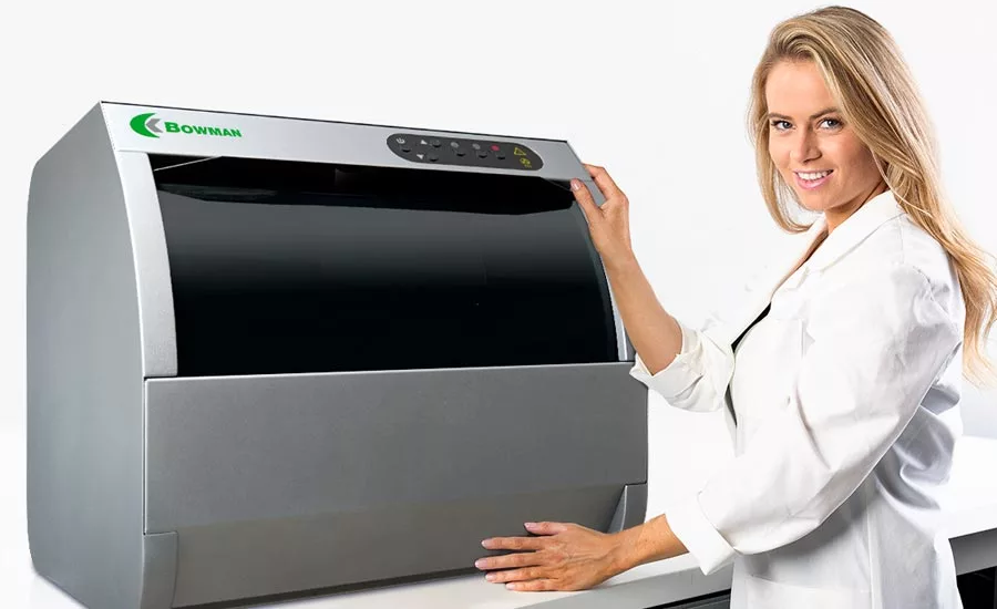
This XRF coating thickness measurement instrument accommodates samples up to 22” x 24” x 13” (LxWxH). It is manufactured with an Si PIN or Silicon Drift Detector (SDD).
Electroless nickel (EN) is industry’s most common plated finish. It’s widely used for applications that demand wear resistance, hardness and corrosion protection—particularly if parts have complex geometries. It is also used in PCB manufacturing within a process known as ENIG, electroless nickel immersion gold.
EN is most valued by manufacturers because it is electro-less—and thus does not need electricity to run—and because deposits are highly uniform: EN plates evenly regardless of substrate shape. This is an important advantage over electroplating, which is subject to flux-density issues due to the electromagnetic field, which shifts with surface profile. It also has a wide deposition window: from 10 microinches to about 4 mils.
Electroless nickel is either nickel phos or nickel boron alloy. In either case, the percent of phosphorus in the reducing agent is a metric whose importance can’t be overstated. EN is, in fact, classified by its phos content: low at 1-4%, mid at 5-9% and high at 10-14%.
Quantifying phosphorus is critical to EN plating primarily because of its direct effect on corrosion performance, and on hardness. The exceptional hardness of low-phos EN (typically 500-720 HK) has made electroless nickel a popular replacement for chromium. (To put this in context, the hardness range of electrodeposited nickel is 150-400 HK.)
Many platers don’t test for phos content in-house, however, relying instead on their chemical suppliers or an outside lab. What they often don’t realize is that phosphorus can be quickly and precisely measured with XRF, a proven and familiar quality tool—if the instrument has the right detector.
XRF systems use one of several types of detectors. Among the most popular for the measurement of coatings are Silicon PIN diode detectors, which deliver spectral resolution superior to the “prop” (proportional) counters that preceded them, so thinner deposits and lower concentrations can be measured, along with multi-layered samples and samples involving “mystery” materials. Silicon PINs combine low noise, excellent resolution, low detection limits and high stability. They are “standard” for most XRF equipment lines, but they are unable to measure phosphorus.
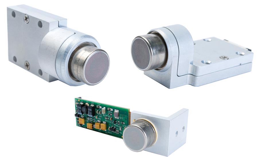
XRF analyzers with silicon drift detectors are ideal for measuring electroless nickel and other coatings. They combine low noise, optimized charge collection, and high uniformity from detector to detector.
Silicon drift detectors (SDDs) are widely preferred for the measurement of coatings. Their count rates and spectral resolution are highest by far; they are best at detecting very low kV photons. SDDs offer substantial peak-to-background ratio improvement over the alternatives, particularly when they are paired with an X-ray tube that uses optimal target material. They can also measure phosphorus, and everything else on the periodic table between sodium and uranium. The only downside is their higher cost.
For a plater that wants—or whose customers demand—verifiable phos numbers, the SDD is a slam-dunk. For shops that envision more—or more tightly specified—EN in the future, there’s a conundrum: make the added investment now, or wait.
Fortunately, there’s a new middle ground. Companies can opt for a lower cost XRF with an Si PIN detector—a system that will measure every major industrial element except phosphorus—and, if and when it becomes important to measure phos precisely, or inline (or at least in-house), swap-out the Si PIN detector for an SDD.
Modularity is not revolutionary (remember Motorola’s “works in a drawer?” No?) but it is new to this application. Upgrading to an advanced new SDD has become more attractive as costs have declined over time.
But let’s consider an alternative view. Some platers (you know who you are) say “we pretty much know where we are on phos, and it doesn’t vary that much. So it’s fine to measure once or twice a month.” (This is an actual quote.) Others acknowledge that routine measurement would be advantageous, either to prevent rejects, or to allow the quoting of a broader range of more lucrative, albeit tighter spec, programs.
In electroless nickel, phosphorus is in solution with the nickel; the elements plate simultaneously. Notably, if you have an XRF that can’t measure the phos percentage, you have to then “tell” the XRF unit what you think the percent phos is for it to function. So, you have to know it, or assume it—and either way, commit to that number.
So, you’re entering a number without knowing it’s valid? In a competitive environment where precision is increasing, this seems unwise.
Components used throughout automotive, aerospace and heavy construction—and the printed circuit boards that run virtually everything—depend on electroless nickel to function, and to last.
And here’s another common scenario: companies send samples for testing, and they come back with a reading of, say, 9.5% phosphorus. But there’s a place-holder for 8 in their calibration and often, no one bothers to change it. (“It’s close enough!”) The difficulty here: a 1% difference in phos translates to a 3-4% difference in EN thickness, and that’s often sufficient to produce rejects.
If you’re doing electrolytic nickel plating, the density of that nickel coating is essentially the density of pure nickel. But when you are doing electroless nickel plating, you’re plating a nickel-phosphorus alloy. The density of phosphorus is 1.8 gm, vs. 8.9 for nickel. The nickel phos coating will have a vastly different density. You can calculate the density of that alloy, and for every 1% phos, it’s about a 3% difference in density, translating to a 3% difference in actual plated thickness.
That’s why knowing the real number is important.
Adam Hammond is technical director at Metal Surfaces Inc. (Bell Gardens, CA) with responsibility for quality operations. He offers this insight: “In electroless nickel, phosphorus is the key determinant for magnetism and corrosion resistance. Percent phos also impacts a variety of other properties such as deposit stress, and electrical resistivity.
“Electroless nickel deposits with significant phos content are nonmagnetic, even though nickel itself is magnetic. So for military and other programs where magnetism is undesirable, high phos EN is an answer—but you must have good process control to maintain the correct % phos, and be able to validate your results.
“The industry overall is becoming more prescriptive, with more oversight and tighter flow-down requirements—oftentimes tighter than the primary specs. So if you have a spec that calls-out mid-phos at 5-9%, it is common to see a purchase order or blueprint that supersedes it. It’ll flow down 5-7% or 6-8%, a much narrower range. In these instances, the spec defines the majority of what the engineer or buyer needs; focus can then be placed on a few parameters that need to be controlled more closely.
“If there are forming operations after plating, like crimping or bending tabs, an engineer or buyer who uses electroless nickel and understands its properties and how phos content can impact them has great deal flexibility in part design and can tailor flow-down requirements accordingly.”
So why not plate electroless nickel with high phos as the default? One reason relates to processing constraints, another to deposit properties. High phos deposit rates are typically the slowest at roughly 300-500 microinches per hour. With mid-phos, you can expect as high as 1,000 microinches per hour, so absent a spec to the contrary, the plater may choose the lower phos option to accelerate throughput.
Regarding the plated deposit, despite the advantages of high and mid phos EN, lower phos is harder, both as-plated and following specific heat treat operations.
Looking for a reprint of this article?
From high-res PDFs to custom plaques, order your copy today!


