Sponsored Content
White Paper: Limitations of 2D X-ray Inspection
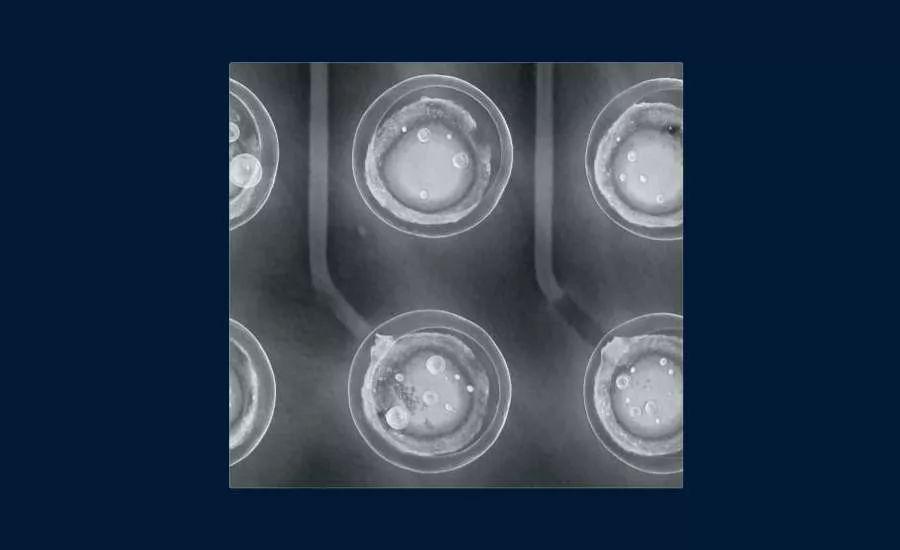
While x-ray inspection of electronics has existed for several decades, the continuous shift in electronics design and manufacturing to smaller, more dense products, is driving x-ray technology forward.
A simple high-resolution x-ray image often provides enough information to process a Pass/Fail decision, quite often the high-density “double-sidedness” of modern circuitry prevents this. This challenge led the inspection industry to an x-ray technology that allows the user to separate top from bottom layers: Laminography.
Looking for a reprint of this article?
From high-res PDFs to custom plaques, order your copy today!


