Vision & Sensors | Trends
Developments in UV and IR Imaging Technology
Recent advancements in sensor and optics manufacturing technologies for UV and IR wavelengths have made imaging systems for these wavelength ranges more accessible.

Source: Edmund Optics
As of recent years, the demand for machine vision systems that capture information in the ultraviolet (UV) and infrared (IR) spectral ranges has increased as more integrators and end users venture into new application spaces. These imaging techniques take advantage of unique light-matter interactions outside of the visible spectrum. The span of applications and industry spaces for these imaging techniques includes package or label inspection for the food and beverage industry, hyperspectral imaging and multispectral imaging for environmental monitoring and agriculture, material sciences and semiconductor inspection, and so many more. Even though imaging out in these spectral ranges is recently less cost-prohibitive and more accessible, many of the design and manufacturing approaches for camera sensors and optical lenses are the same and the same technological advances that drive down costs associated with these more novel applications are improving visible imaging system technologies as well. However, there are several key differences in the technology for both UV and IR imaging.
Camera Sensor Technology
Camera sensors are an array of pixels that consist of a semiconductor photodiode substrate, metal wiring, and a microlens array. Seen in Figure 1, there are two main sensor architectures, both with a different order to the orientation of the constituent layers. Backside illuminated (BSI) sensors as show in Figure 1 A) feature superior signal-to-noise ratios and more even illumination across the entire sensor than frontside illuminated (FSI) sensor, shown in Figure 1 B), as the incident light has less depth to penetrate for a BSI sensor than for an FSI sensor.
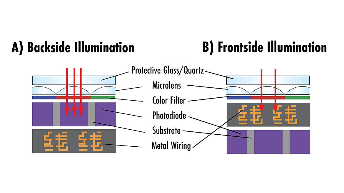
The manufacturing of sensors for UV and IR sensors is nearly identical to that for visible (VIS) sensors save for the addition of a protective quartz top layer for UV sensors, which replaces the typical glass in visible sensors due to its transmissive properties in the UV. However, the material used to construct the photodiode substrate may also differ for sensors required for particular or broader wavelength ranges.
The photodiode substrate is the part of the sensor where incoming photonic signals are converted to electronic digital signals to be offloaded to a computational unit for image construction. Each photodiode substrate material has a particular sensitivity to light at different wavelengths. This sensitivity is often reported using a quantum efficiency curve and it is a measure of the efficiency for a sensor to do the photon-to-electron signal conversion as a function of wavelength.
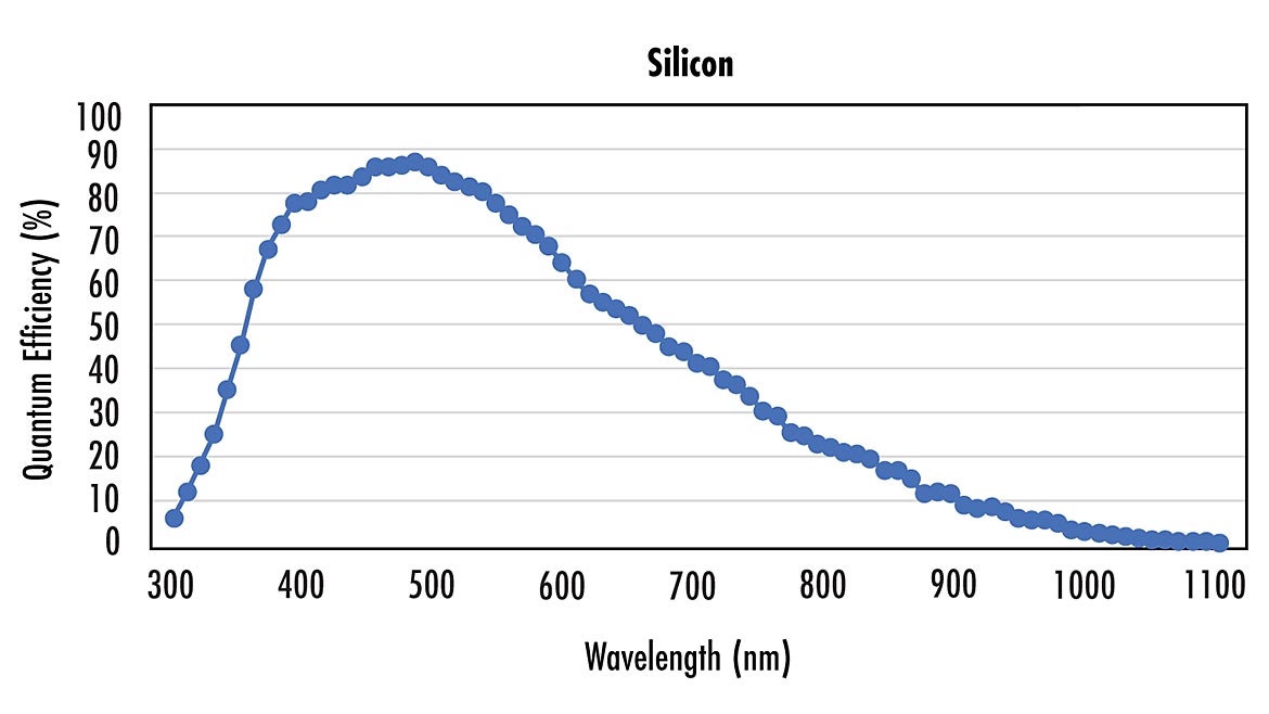
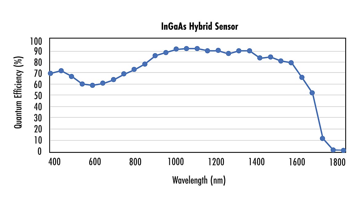
The material used for the fabrication of the photodiode substrate on machine vision cameras for VIS and UV spectrums is typically silicon due to the quantum efficiency being exceptional for VIS and decent in the UV. Silicon also remains relatively sensitive out to the shorter IR or near-infrared (NIR) wavelengths (0.75µm - 1µm) so it is typically used for VIS-NIR sensors. However, silicon is a poor material to use for wavelengths beyond NIR including short-wave IR (SWIR) between 1.4µm to 3µm, mid-wave IR (MWIR) between 3µm to 5µm, and long-wave IR (LWIR) up to around 14µm because of its band gap at 1.1 um. For this reason, IR sensors used for SWIR wavelengths are constructed of materials such as Indium Gallium Arsenide (InGaAs).
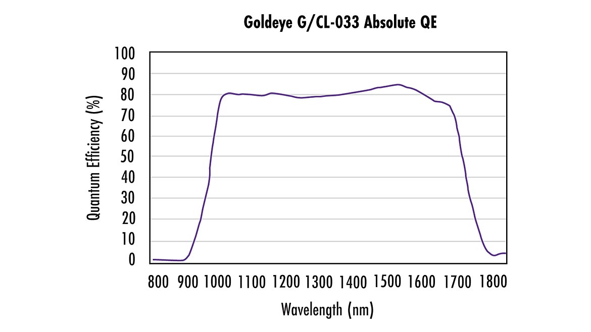
Hybrid sensors for VIS-SWIR (400nm – 1700nm) and NIR-SWIR (700-1700nm) imaging are typically constructed from InGaAs. Some manufacturers make use of particular technologies for sensor fabrication as well. Most IR sensors contain a layer of Indium Phosphide (InP) of various thickness overtop the InGaAs substrate for the rejection of undesired short wavelengths. By changing the thickness of the InP layer, wavelength rejection is specifically attenuated. The InP layer on many of Sony sensors is thin enough to pass visible wavelengths for hybrid usage. Sony also makes of use of a particular manufacturing technique for hybrid sensors called copper-copper (Cu-Cu) hybridization or bonding which happens at the pixel level to bond substrates of different materials [2].
UV And IR Optical Materials For Lens Design
Because the majority of machine vision imaging is done in the visible spectrum, there are many different types of optical glass material available for these optical lenses and less materials in general available for the IR and UV. Optical glass can be creatively used to fit many NIR and SWIR applications but LWIR and UV imaging applications require exotic ionic or metallic/metalloid crystals.
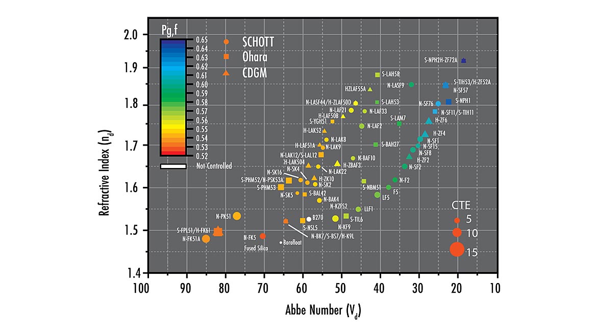
The glass chart in Figure 5 shows the sheer number of optical materials available. Most materials on this chart are optical glass: crown (Abbe Number of >55) and flint (Abbe Number of <55). these glasses and some others including fused silica may only offer utility for nir even swir wavelengths but typically fail in optical designs meant uv, mwir, lwir wavelengths. materials use swir, applications are limited availability therefore more expensive to use. ionic halide chalcogenide crystals (e.g. al2O3 or sapphire,BaF2, CaF2, KBr, LiF, MgF2, NaCl, ZnS, ZnSe, etc.), as well as metalloids including silicon (Si) and germanium (Ge). 55).>
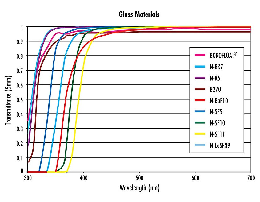
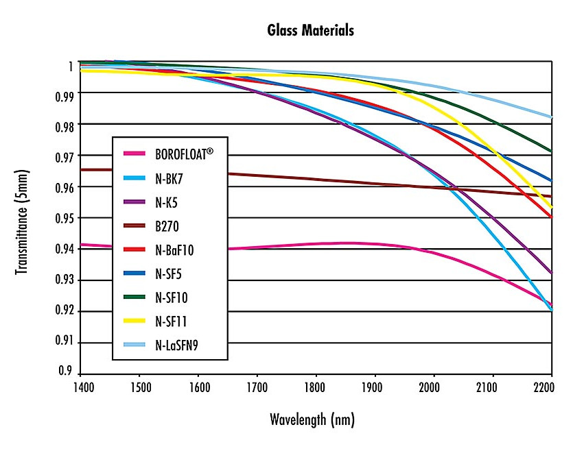
Selecting appropriate materials for optical imaging lenses usable in the UV and IR wavelength ranges requires careful consideration of the transmissive, autofluorescence, and thermal properties of materials in the ambient environmental temperatures of the specific application use cases. One representative application example is thermal imaging which requires the use of optical materials with ideal optical properties in the LWIR. As wavelengths increase, available materials for consideration become fewer. The materials appropriate for UV applications are even less numerous than those for IR applications seen in Figure 6, as typical optical glasses will not be suitable. UV applications mostly rely on expensive crystalline materials [3].
UV radiation also inherently presents two specific unique challenges: solarization degradation of products and energetic danger to human operators. UV radiation is higher energy and therefore more dangerous than visible and IR radiation and thus safety precautions as well as proper failure mode and effect analysis (FMEA) must be considered for safe application conduct.
Testing & Metrology
Vision & Sensors
A Quality Special Section
Testing designs for the UV range is also difficult as there are few high-precision, high-accuracy sensors and UV radiation sources available for commercial production. Additionally, the same dangers and damaging effects that UV radiation present to end users and application hardware are also present to operators, technicians, and analysis equipment during testing. Thus, capital costs, operational costs, and maintenance costs for highly specialized UV equipment are also more expensive than for standard equipment.
Seeing Is Believing
Recent advancements in sensor and optics manufacturing technologies for UV and IR wavelengths have made imaging systems for these wavelength ranges more accessible. However, these sensors and optical lenses have very specific design requirements and the constituent components are made from much more expensive and more exotic materials than components for the visible spectrum, driving up the price for this hardware. Given these design challenges and the increase in the magnitude of costs associated UV and IR applications, it can still be more efficient to use machine vision components designed for the visible spectrum whenever possible as clever optical design techniques can often prevent end users from needing to venture into more challenging and expensive wavelength ranges.
Sources:
- “Detail”, Allied Vision. [Online]. Available: https://www.alliedvision.com/en/camera-selector/detail/goldeye/cl-033-tecless/. [Accessed: 5-May-2023].
- V. Koifman, “IEDM 2019: Sony SWIR Imager”, 20-Jan.-2019. [Online]. Available: https://image-sensors-world.blogspot.com/2020/01/iedm-2019-sony-swir-imager.html. [Accessed: 5-May-2023].
- “Optical Glass”, Edmund Optics. [Online]. Available: https://www.edmundoptics.com/knowledge-center/application-notes/optics/optical-glass/. [Accessed: 5-May-2023].
Looking for a reprint of this article?
From high-res PDFs to custom plaques, order your copy today!


