NDT | Computed Tomography
The most effective and precise battery inspection technology
It’s the tiniest defects that are the major problems today.
All images Source: Comet Yxlon
X-ray and CT technology has long been indispensable as a nondestructive testing method for industrial applications. It is developing as rapidly as the industries using it. And more and more sectors are discovering the advantages of X-ray technology. In particular, the current increase in e-mobility with its high demand for batteries and the requirements on the semiconductor industry to develop and produce even smaller and more powerful microchips bring challenges to which 3D X-ray technology can be the answer.
Additive manufacturing discovered very early on that computed tomography is a valuable companion already in the development of new products and new materials. Both based on 3D, AM and CT work hand in hand. For example, volume data from a computed tomography scan can be the source for additive manufacturing to reproduce existing objects or develop prototypes. Much more important, however, is the inspection of 3D-printed components using CT to check the internal structures for quality and functionality, such as the permeability of internal channels, porosities, wall-thicknesses, or powder residues.
Regardless of whether 3D-printing or conventional manufacturing methods are applied, CT data offer manufacturers an immense wealth of information that provides knowledge about the flawlessness and performance of the product and, moreover, about their manufacturing process. They enable targeted process optimization and increased productivity. Using the full range of image processing technologies such as computer vision and machine or deep learning, a wide range of supporting software solutions is available for different usage scenarios - from software-based evaluation to fully automated defect recognition (ADR). With the help of automatic data transfer, image acquisition, CT reconstruction, visualization, analysis tools, data processing, statistics, reporting and archiving tools are integrated with each other in the system, providing comprehensive information to the manufacturer that can get directly used for product and process optimization. An interface to the user network enables further processing and archiving independently of the inspection system.
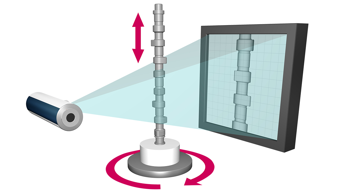
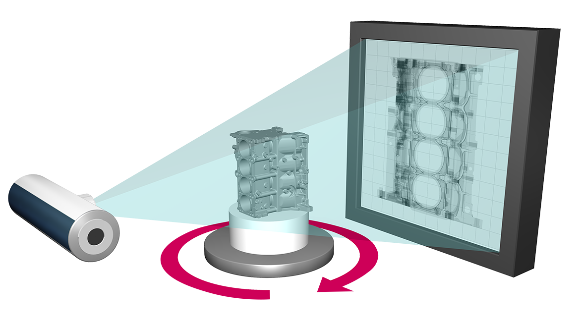
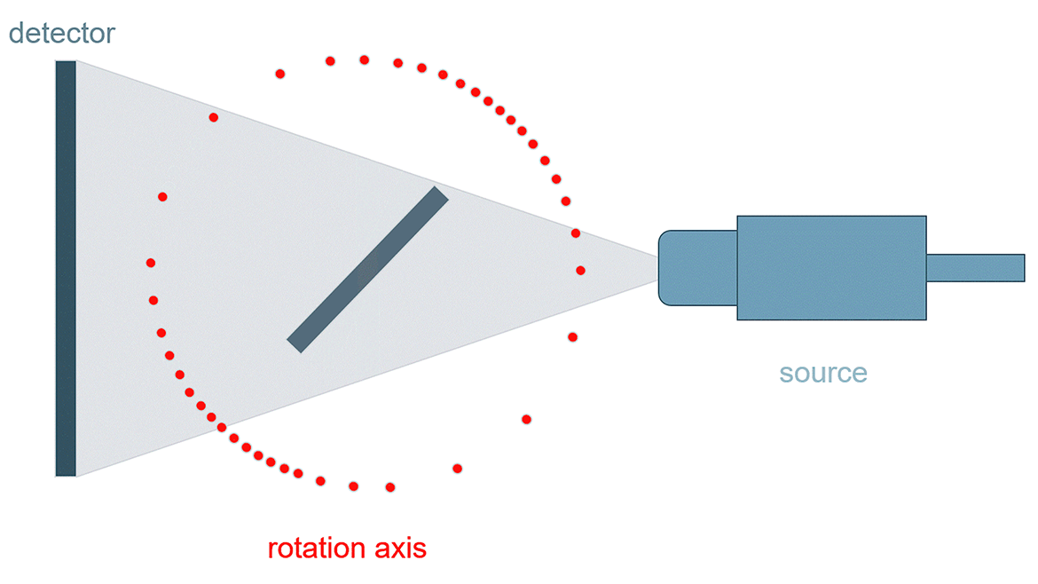
On the one hand, the optimal selection of X-ray components, such as a stable tube with the appropriate power and focal spot, a high-resolution detector, and also a solid, precise manipulation system are the basis for high-quality images. On the other hand, the scanning technique, i.e., the selection of the optimal trajectory for the respective inspection part, has a significant impact during the inspection process and on the results. In the following, we refer to the most commonly used cone-beam CT with a flat-panel detector.
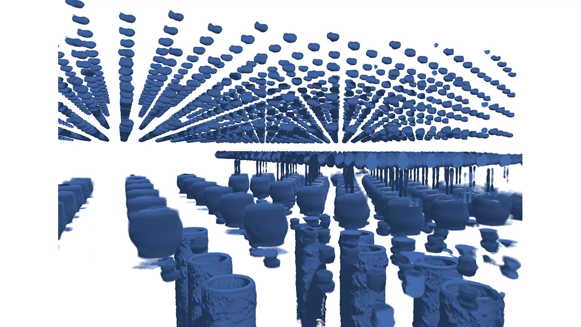
In a circular scan, the test object between the radiation source and detector is captured during a 360° rotation from all angles with hundreds of 2D images in a single plane. In a helical CT, the rotation of the test object is combined with a vertical movement so that taller objects can get captured in one scan. If the parts are also wider than the field of view, two offset helical scans can be performed and added them. All trajectories are usually available in two modes: a high-resolution quality scan with stop-and-go rotation and a quick scan with continuous motion. The choice depends on the requirements of the inspection task: Do I need a 3D CT volume with the highest resolution for a detailed analysis, or is a fast overview scan sufficient to define the regions from which I want to make additional high-resolution detail scans? Planned, optimized inspection processes according to individual requirements ensure maximum efficiency in an inspection method whose possibilities seem almost limitless.
Maximum efficiency is currently most vital in e-mobility. The demand for high-performance batteries is rapidly growing. More and more battery production facilities are getting built worldwide, and with them, an enormous increase in the need for inspection. Various testing procedures are applied in both R&D and production of batteries, not just to ensure their quality, function, and performance, but for safety aspects. Faulty assembly or a leaking housing, e.g., can lead to a short circuit and even fire in a battery cell, which would trigger a fatal chain reaction in a tightly packed battery system. Accordingly, regardless of the format of the cell, extensive inspections are required, focusing on possible deformations, the welds, anode overhangs and their correct alignment, potential fractures, delaminations, pores, foreign inclusions, and more.
The most effective and precise battery inspection technology is 3D X-ray, which makes the internal structures visible through the housing. Battery cells or entire modules already installed in devices can even get reliably examined without having to be removed or opened.
Modern analysis software uses artificial intelligence for automatic scan data evaluations, for example, when checking and measuring the anode overhangs and their alignment. These automated analyses don’t only make an inspector’s life easier and are faster than manual inspections. They also ensure objective, consistently precise, and repeatable results at any time – the basis for maximum reliability.
NDT
Related Article
With 3D X-ray technology applied as early as in the research and development stage, many problems in the subsequent production process can get avoided, as it reveals important information about the design of the part, the raw materials, and the correct implementation of the planned geometry maximally reducing costly scrap, saving valuable raw materials, and increasing yield.
There are three cell formats commonly used in e-mobility today: the cylindrical battery, the prismatic battery, and the pouch cell. The aspect ratio of flat prismatic and pouch cells is unfavorable for circular CT scans because the longest edge of the test part dictates the distance to the tube, and, thus, only the two side edges get close enough to the X-ray source for the best resolution. That means that optimal scan resolution for the entire part cannot get achieved with conventional CT.
Two breakthrough features on the market allow for the efficient inspection of such flat objects: Using a special software, you can define the exact outline of the test part, in this case, the battery cell. Basically a reliable collision protection that safeguards your valuable inspection parts as well as the system components, it enables the accurate positioning of the part for optimal scan resolution and magnification. Combined with a zoom scan, the system precisely follows a trajectory at this outline, maintaining an optimal distance to the test part. This method achieves the maximum resolution for a defined region of interest.
Since time is of the essence, a specific speed mode can be combined with this zoom scan feature in the case of such parts. The flat sides of the battery contain the fewest information and, therefore, do not require as many captures as angled perspectives or thicker areas. With this mode, you can define the scan steps, i.e., broader steps at regions with little information and smaller steps, i.e., more shots at the more information-rich positions. This way, you can significantly accelerate the inspection process while keeping the image quality high and without additional undersampling artifacts.
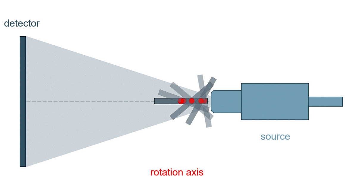
But another technique for scanning flat parts offers even higher detail resolution which is so vital in the semiconductor industry and is, therefore, considered the future of semiconductor inspection: computed laminography (CL). For such flat areas, CL requires much less projections than CT. As a result, the inspection time is significantly reduced even though the resulting inspection volume is just as high in quality. Since CL does not require the 360° rotation of the part, it is not prone to common photon starvation artifacts which is a benefit to many applications for example, when examining critical junctions such as solder bumps and TSVs (through-silicon vias). Each layer can be analyzed individually, or as a full 3D volume. This 3D volume, in turn, can be sliced in any direction and examined in detail. In doing so, computed laminography is much faster than, for example, FIB-SEM (focused ion beam scanning electron microscopy) and in most cases detailed enough to detect all critical defects. Today’s CT/CL inspection systems ensure consistent image quality and stable, repeatable results even after hours of operation during batch inspection. Automated image analysis provides reliable results and increased efficiency.
As a consequence, 3D X-ray inspection using computed laminography establishes itself as a tool for production monitor. It is becoming a real game changer in the semiconductor industry. The main pains of manufacturers - long ramp-up processes, high and costly scrap, long time-to-market, and finally late ROI - are all combated with this best-in-class 3D X-ray technology. With computed laminography, the zero-defect goal is within reach.
Looking for a reprint of this article?
From high-res PDFs to custom plaques, order your copy today!


