XRF Analysis: What Labs and Lines Really Want—and New Features That Get Them There
Everyone’s ultimate goal: minimal variation, maximum speed.
This “bottom-up” XRF uses a motorized Z-axis with laser auto-focus.
Innovations in the electronics and semiconductor industries have birthed two relentless trends. Both profoundly impact both product designers and those charged with assuring that what was designed is what was manufactured. The trends are: higher densities for components, boards and processors, and the need for very high precision in the metal plating that enables functionality.
Measuring many small features (a wafer with 1,000 features, some of which are less than 100µm is no longer an anomaly) and quantifying multiple metal plating layers is usually tasked to XRF systems. For every company, the objectives are threefold: to do and document as much testing as practical, to minimize errors from operators or equipment, and to maximize efficiency through tools such as “travelers,” which track a sample’s ID throughout manufacturing and testing.
Analysis is often done both in-line (following various stages of production) as well as in the lab. The wants and needs of those diverse camps have resulted in a series of innovations that benefit both. Here are the six most notable:
Polycapillary X-ray optics
Polycapillary optics is comprised of hundreds of thousands of stand-alone glass channels that collect a large solid angle of X-rays emitted from a diverging source. The X-rays pass through the optics by total internal reflection and are focused to a small spot with ultra-high intensity. Typical intensity gain compared with the mechanical pin hole aperture (collimator) is more than 1,000 times. These optics also deliver a very clean excitation beam, compared with a collimator, and an extremely well-defined focal spot. The most advanced XRF systems have a spot size of 7.5 microns, allowing them to measure the smallest features, down to less than 20 microns in diameter. As a bonus, polycapillary optics enables very short test times.
Z Protection with laser scanner
As samples are positioned on the X-Y-Z stage, the scanner’s laser powers up and scans for intrusions; it stops when the laser detects the sample. The process then repeats to cover the remaining sections of the stage. The table retreats to the highest point at which it stopped, and executes a slow scan, establishing the Z travel range. The X-ray head approaches this position, and the “No Part Loaded” message switches to “ready,” signaling the process is complete. Subsequently, the head will be unable to move below the position where the sample was located, preventing contact by restricting Z axis travel.
This micro XRF uses poly-capillary optics to focus the X-ray beam to 7.5 µm FWHM, the smallest beam size for coating thickness analysis using XRF technology.
Laser Auto Focus
When measurement tasks were simpler, optical focusing was sufficient for positioning samples. Today, with the definition of “precision” continuing to evolve, the roughness of a sample surface often creates an issue, since it easily confounds the auto-focus of an optical device. Technology’s answer is the laser focus. When activated, all of the lights in the unit turn off, and the software seeks the center of the laser which is calibrated at a fixed angle to define the working distance. When located, the software moves the Z-axis to the center of the laser for precise and consistent measurement distance. This feature ensures that samples are within a few microns of the in-focus position for greatest accuracy. Bonus: it does so in two seconds or less.
Pattern Recognition
Much like voice recognition, pattern recognition isn’t new, but, like other instrument features, has substantially evolved in recent years. Advanced pattern recognition enables fast, highly precise determination of the measurement locations for even the smallest structures. The software corrects the XY position whenever the X-ray beam is not 100% within the boundaries of the feature. (One might say it’s great to be “leading edge,” but not “on the edge.”)
Image details or patterns are set using a recognition menu. The software then compares the measurement location with the standard. It is also possible to define multiple image details or patterns in order to obtain automated measurements on structures. This prevents errors from operators programming incorrect locations or from the sample stage not moving to the precise location of the small features.
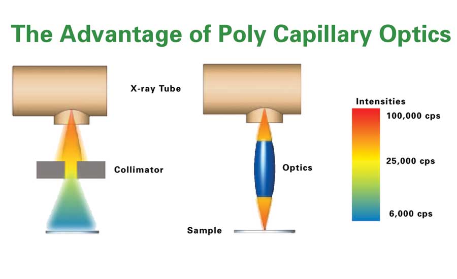
Polycapillary optics accelerates photon counting. Illustration credit: Bowman
Barcode Scanning
Using integrated magnification cameras, the software reads both 1D and 2D bar codes. These codes are stored in the database with the readings, or used to select a file for sample analysis. This feature is important where automation and error minimization is critical to ensure sample traceability. The barcode is able to “teach” the XRF which program to select for analysis, and what labels (serial #, lot #, etc.) are to be stored with the data collected.
Standardized API for automation and data transfer
Automation API allows system integration with customer SCADA systems. Sample code and documentation is supplied for system integrators, allowing the user to write program logic and database interfaces to fully integrate the XRF system into an existing operation. With minimal knowledge of the inner control codes for the XRF system, the end user has full control of measurement operation and sample measurement data to integrate with SAP, SEMI SECS-II or other systems.
Looking for a reprint of this article?
From high-res PDFs to custom plaques, order your copy today!


