LED Light Pulses Enter the Nano Realm to Keep Pace with High-Speed Imaging
A competent vision designer can optimize image capture at extremely high speeds.
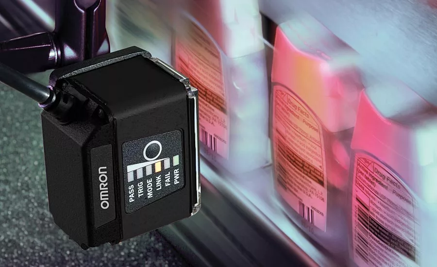
Quality assurance during high-volume production operations, such as the inspection of consumer packaged goods (CPGs), is possible only through the application of high-speed machine vision systems.
Quality assurance during high-volume production operations, such as the inspection of consumer packaged goods (CPGs), is possible only through the application of high-speed machine vision systems.
While the meaning of “high speed” may seem self-evident, in the context of machine vision, the term has no fixed definition independent of the application. It simply means that the system can perform accurately and consistently without becoming a bottleneck on a high-throughput process.
In practice, creating a high-speed system involves design considerations, including camera trigger latency, how field of view (FOV) influences shutter speeds, and short exposure times to freeze rapidly moving objects in time. Proper illumination is another important factor, as it can help ease or even eliminate other system design considerations.
Traditionally, xenon strobes or pulsed LED light sources have been the favored solutions for freezing part motion in high-speed imaging applications. Xenon flashlamps are brighter in terms of absolute photon output, and their light pulses when strobed typically last from 15 to 30 microseconds (µs), though they can pulse as low as 250 nanoseconds (ns) if necessary. To date, the shortest pulses that LED lights can effectively deliver are in the low microsecond range.
As solid-state light sources, however, LEDs offer several advantages over xenon lamps. In addition to greater ruggedness, lower maintenance, and longer lifetime, LEDs afford better control over the duration, intensity, and shape of the pulse. Moreover, the absolute intensity of a light source has less bearing on image capture than the flux density—the number of photons per unit area projected within the target FOV per one second of time. This gives LEDs additional practical advantages versus xenon sources. For example, LEDs can emit at a narrower spectral range, which often enhances the contrast and visibility of key features in
an image.
The comparatively compact form factor of LED lights also enables them to be positioned closer to the target. The inverse square law states that intensity decreases in proportion to the square of the distance. This decline relative to distance permits smaller LED heads positioned nearer the target to overcome their lower absolute intensity versus xenon lamps. In practical terms, this means they can achieve comparable or even better illumination compared to xenon sources and higher flux density across the FOV.
Today we are seeing the emergence of advanced LED driver technology that is enabling light sources to deliver excellent pulse control and high intensities in sub-microsecond time frames. The introduction of such drivers promises new possibilities for improving the performance and/or rate of high-speed inspection operations.
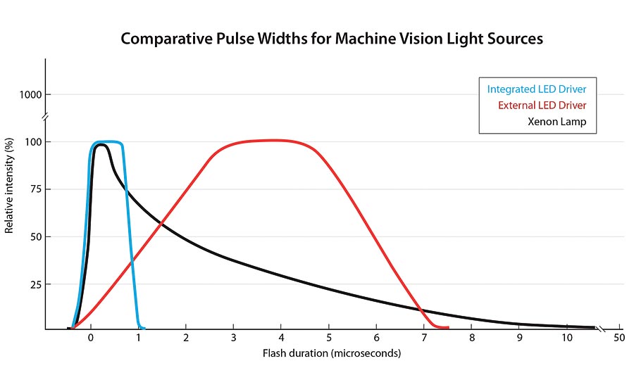
The shape of a light pulse is as important as its absolute intensity. Though xenon lamps (black line) can emit comparatively higher intensities and shorter (25 µs) pulses than LEDs, only 10% of their light is effective due to poor pulse control and fast off times. LED sources with external controllers (red line) are capable of emitting more controlled pulses than xenon sources, in the nanosecond range. However, inescapable parasitic impedances of external wiring contribute to broader pulses with sloped edges, resulting in system jitter (shaded area) and blurred images at fast exposure times.
Contrast the performance of these sources with the controlled pulse shape from LED designs (blue line) that integrate driver and controller in close proximity on the motherboard. This architecture eliminates impedances from wiring and allows the LED to achieve full power in the 300 to 500 nanosecond time frame and deliver repeatable, high-intensity pulses with durations in the microsecond range.
Freezing Time
A vision system’s ability to freeze motion in an image is a function of how precisely and quickly it can put photons to pixels. The faster the motion, the more challenging this becomes. A common goal is for each pixel of a camera sensor to detect one point on an object. If the point is moving too quickly relative to the camera’s exposure time, it may be captured across multiple pixels. The resulting pixel blur causes poor image data. The best image quality will limit pixel blur to one pixel or less.
This level of performance is not always necessary. High-speed inspection applications often specify the allowable threshold for pixel blur, and vision engineers design systems accordingly. There are two fundamental—and complementary—approaches to design. Traditionally, engineers used the following formula to calculate the minimum exposure time required to avoid a specified pixel blur:
pixel blur = (line speed * exposure time) * (image size/FOV)
So, assuming pixel blur can equal no more than 1, for example, it is possible to calculate exposure time by plugging in other known quantities. If the engineer knows that the line speed is 100 millimeters per second (mm/s), the image size is 640 x 480 pixels (using the pixel count in the direction of travel, or 640 horizontal in this case), and the camera’s FOV is 150 millimeters (mm), then:
1 pixel of blur = (100 mm/s * X seconds) * (640 pixels/150 mm)
This works out to an exposure time of 0.0023 seconds, or 2.3 milliseconds (ms).
Exposure time is one side of the system design coin. Illumination is the other. The faster a feature of interest moves through a camera’s FOV, the more quickly the camera’s shutter needs to open and close to freeze it in time. As shutter speed increases, the target needs to be more brightly illuminated to ensure proper exposure at each pixel.
Widening the aperture of the camera will help it capture more light. But this also results in a smaller depth of field, which is unacceptable in some inspection applications. Similarly, increasing camera gain can brighten output, but this practice also amplifies image noise. Achieving high intensity and even illumination across the scene at short exposure times remains the best solution for machine vision applications in which image quality determines success.
The Impact of Pulse Rate and Shape
Given the limited number of ways a camera system can be tweaked to gather more light during short exposure times, it is advantageous to illuminate the object of interest more intensely. As mentioned earlier, overdriving LEDs at high currents can increase light output, sometimes providing up to 10 times more output than constant operation.
A vision system’s ability to freeze motion in an image is a function of how precisely and quickly it can put photons to pixels. Vision system design typically assigns a certain number of pixels to ensure accurate capture of a corresponding point on a moving object, such as a narrow bar of a UPC bar code. This helps the designer calculate system features such as exposure time, field of view, and the illumination necessary to avoid pixel blur. Source: Omron
As pulse lengths decrease to accommodate shorter camera exposure times, the shape of each pulse—the time it takes the LED to reach full intensity and then switch off—becomes increasingly important. Measured in intensity over time, an LED light pulse should exhibit a square shape, which indicates that the die is achieving full output power more quickly. This ensures that an LED is not still “rolling on” when the camera shutter opens but is rather illuminating the target with its full intensity. Otherwise, pixel blur can begin to creep in.
While delivering full intensity more quickly is necessary to achieve sharp, microsecond light pulses, the key benefit of this capability is greater control and precision when syncing a light pulse to a camera’s exposure time. This helps explain the importance of integrated LED drivers in achieving the practical benefits of the technology. Some high-speed LED systems on the market can deliver pulses in the same microsecond duration using external controllers. However, the physics of such systems introduces inescapable latency issues that dull the edge of that square pulse shape. The longer the cable, the greater the impact from latency. Even a two-foot cable connecting driver and light source will impose significant parasitic impedances that contribute substantially to system jitter and extend the rise to full intensity into the microsecond range.
Designing Nanosecond LED Drivers
Integrating the driver and controller in close physical proximity to each other on an LED’s motherboard eliminates the need for external wiring and ensures that high-current pulses from the driver are delivered directly to the LED across comparatively short, impedance-controlled PCB traces. Such integrated driver designs minimize the resistance and parasitic electrical losses from external cables and underlie the development of LED light sources capable of quickly delivering tens of amps to the die to achieve full power in 500 nanoseconds (ns) or less with comparable off time. Applied to high-speed imaging, these light sources permit incredibly short image acquisition times and precision timing that would be impossible to achieve using LED sources driven by external controllers and wiring.
LEDs powered by this advanced new driver technology can be configured to enable sub-microsecond pulse edges to maintain 1 µs pulse widths. With a 10% duty cycle—meaning the light is on only 10% of the time—such lights can conceivably achieve 100,000 strobes per second (SPS) at maximum output.
Additionally, faster on/off rates help compensate for latency issues during asynchronous operation, wherein a camera shutter is triggered by an external source, such as an approaching product tripping a photosensor.
The higher pulse rate and better control of these emerging LED drivers promises to enable quality assurance inspections at substantially higher throughputs.
Nano Pulses in Practice
Consider a high-speed application in which the camera must scan UPC or EAN-13 bar codes on parts moving up to 150 inches (3.8 m) per second, with a rate of up to 50 parts per second.
Assume that the narrow bar width is 13 mil (0.013 inches) and that at least two pixels per thin bar are assigned to capture it for consistent decoding. However, to further ensure consistent decoding at such speeds, the tolerance for pixel blur is established at 0.5 pixels.
These specifications translate to an image pixel size of 0.0065 inches and a desire to keep motion-induced blur under 0.00325 inches. At 150 inches per second, the narrow bar of the code would traverse that half pixel within 0.0000216 seconds, or 21.6 µs.
Accurately scanning codes without pixel blur at that speed is a challenge with conventional cameras, which have a minimum exposure time in the range of 50 µs or longer. The minimum strobe durations of externally driven LED light sources present a further hindrance to such fast exposure. Not only will parasitic cable impedances limit resolution to the microsecond range, but such sources offer limited ability to deliver significant current for short intense bursts.
All these issues can be resolved by an LED driver that delivers full power with rise and fall times under one microsecond while allowing tens of amps to reach the LEDs for the main duration of the pulse. The duty cycle of such an LED design would exceed 50 pulses per second.
Conclusion
For all the sophistication underlying built-in LED drivers capable of pulse edge resolution in nanosecond time frames, the end benefit is simplicity. A competent vision designer can apply complex trigger schemes, advanced cameras, or software tricks to optimize image capture at extremely high speeds. Such solutions, however, always face the headwinds of an end user’s cost-benefit analysis.
By enabling shorter, brighter pulses characterized by on/off times in the nanosecond range, new advanced LED drivers will boost both accuracy and throughput for high-speed inspection applications. Importantly, the greater control they afford will also help streamline the design, implementation, and cost of these systems.
The author thanks Omron’s Microscan Group for providing the details relevant for our hypothetical bar-code scanning application.
Looking for a reprint of this article?
From high-res PDFs to custom plaques, order your copy today!


