Computed Tomography’s Role
Accelerating time to market and improving profitability
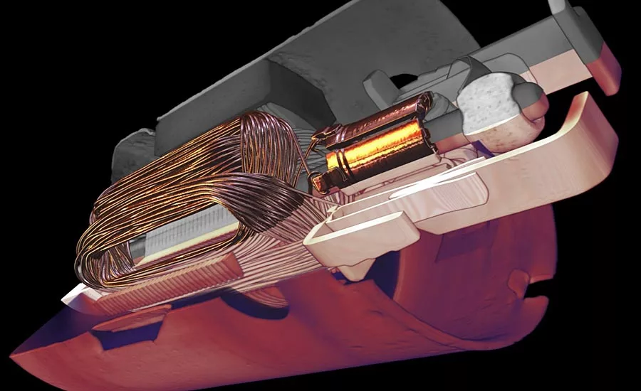
Figure 2. 3D volume of an automotive pump. Source: North Star Imaging Inc.
With the advancements of many manufacturing processes, computed tomography (CT) and digital radiography (DR) are continuing to expand into new sectors of nearly all industries. Historically, these nondestructive testing (NDT) methods were primarily used for inspection of critical components, however, we are seeing an increasing number of companies extensively applying these technologies beyond just inspection work. The value these technologies bring to the development of new processes and products is proving to be extremely valuable. Companies are gaining a better understanding of the true monetary value of reducing time to market for new products. Applying CT early on in new development work provides the advantage of not only quickly identifying problems, but also of having enough information to genuinely understand the root cause of product and process failures that negatively impact a product launch schedule.
The old phrase “We don’t know what we don’t know” really drives the point home that maybe we should consider where it is most prudent to take the time to look deeper. When we do, we often find out not only just where there are opportunities for improvements, or where there are potential catastrophic failures in waiting, but also we provide confirmation of what we are doing really well, where our manufacturing processes are in control, basically, where our strengths are. Both sides of this information can be vital to success. As powerful as DR has been in helping provide pieces of this knowledge, CT provides exponentially more useful information to help remove the factors of what we can’t see, or of what “We don’t know we don’t know.” This knowledge not only helps us produce higher quality and higher performance products, but it helps us drive down manufacturing costs by providing the necessary information for real process improvements.
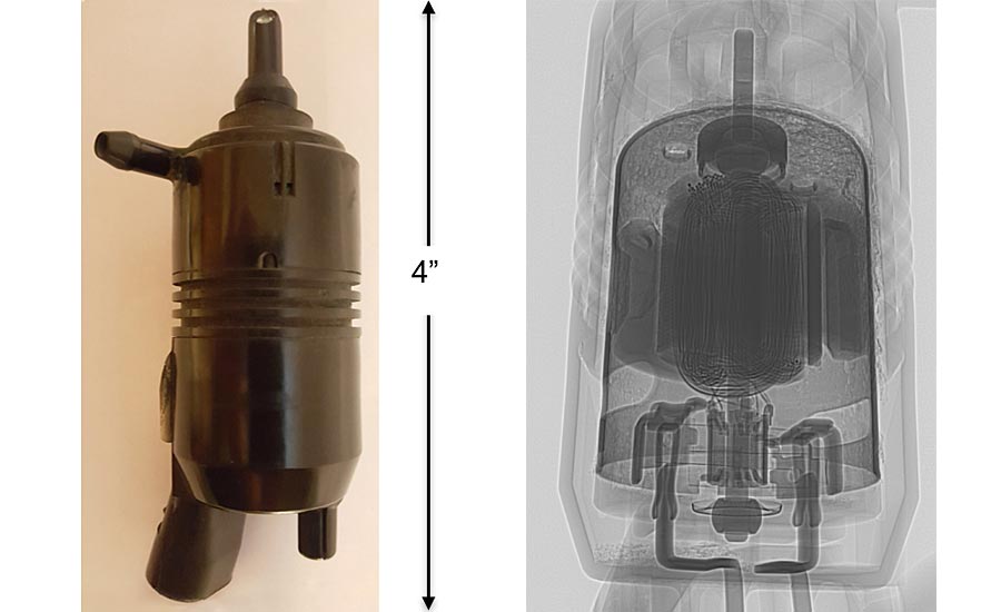
Figure 1. An automotive pump. Source: North Star Imaging Inc.
In Figure 1, we see a 2D DR image of an automotive pump assembly. Even in this high-quality image, the component features are superimposed on top of each other making it more difficult to clearly view specific feature details. In Figures 2 and 3, a 3D CT volume provides tremendous feature details and allows for one to not only slice through the 3D volume from any plane, but also provides for the segmenting of materials, delivering even further individual component clarity.

Figure 2. 3D volume of an automotive pump. Source: North Star Imaging Inc.
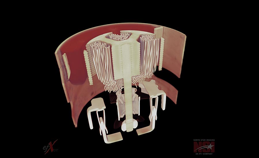
Figure 3. 3D CT of an automotive pump. Source: North Star Imaging Inc.
As we consider the investment in any technology, a question that can easily be overlooked is: What’s the value of accelerating bringing a new product to market while reducing the risk of quality, reliability, or performance concerns? Or, the negative of that is: What is the true cost of a delay in getting a high volume or high dollar product to market due to process or product concerns that could have been caught early with the right equipment? Companies that take a serious look at these considerations can often provide an easy ROI for supporting the investment in CT equipment to help them accelerate product development functions and provide a higher level of assurance of product performance, reliability and safety throughout some of the most demanding markets.
For most products, the most efficient method of continually providing high quality products is not to rely on inspecting quality into products, but rather to develop, qualify, improve, and monitor manufacturing processes over time. CT is currently being used in all of these segments of operation.
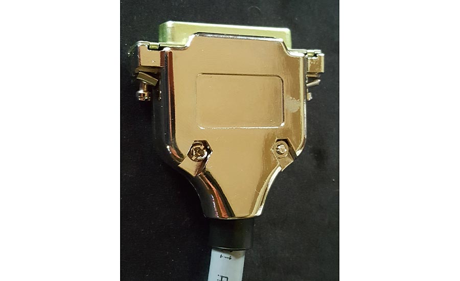
Figure 4. A photo of a 24-pin electrical connector. Source: North Star Imaging Inc.
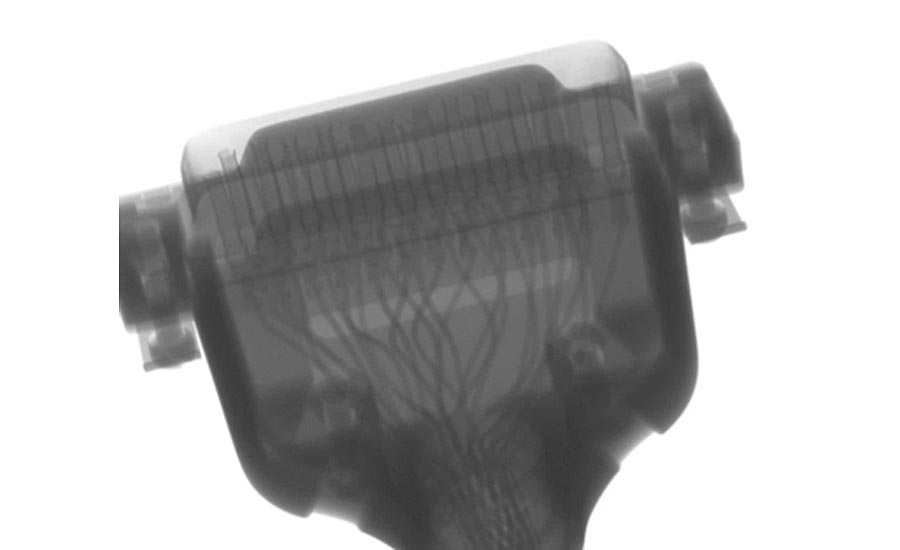
Figure 5. A DR of a 24-pin electrical connector provides a better quality image. Source: North Star Imaging Inc.
Figure 4 displays a photo of a 24 Pin Electrical Connector from an aerospace product application. Once again, a 2D DR image (See Figure 5) makes it extremely difficult to interpret through all the superimposed component information.
Because of this, two to four views are necessary to provide a higher level of interpretation confidence. However, the overall probability of detection of some defect types can still be inferior for certain regions of the part and the interpretation can be time consuming.
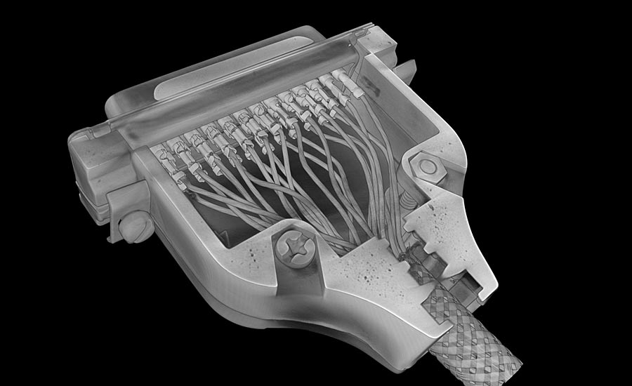
Figure 6. 3D CT volume of a 24-pin electrical connector. Source: North Star Imaging Inc.
Figure 7. 3D CT of a 24-pin electrical connector. Source: North Star Imaging Inc
Figure 6 displays a 3D CT volume that allows one to virtually remove the outer cover and rotate the volume as if inspecting the full part without an outer case.
Figure 7 provides a view of how each row of pins can be segmented out and rotated allowing for each electrical connection joint to be evaluated independently while also looking for stray wire strands and foreign objects or debris within the case. In some industries, there will always be products that will require 100% inspection because of their critical nature and applications where failure is simply not an option. In these cases, CT will typically provide the image quality with the highest probability of detection of the smallest of defects. In many of these applications, CT can still be a high-speed inspection process. For example, the CT scan time for the electrical connector in Figures 6 and 7 was only 15 seconds.
In Figures 8 and 9 Integrated Circuit Chip images, we see another DR and CT comparison that displays an obvious improvement in the feature and defect detail displayed in the CT Data (See Figure 9).
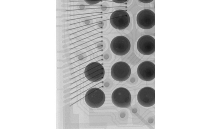
Figure 8. DR of an integrated circuit chip. Source: North Star Imaging Inc.
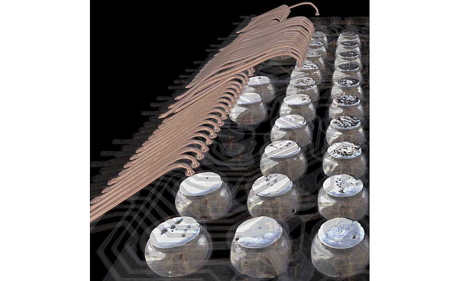
Figure 9. CT of an integrated circuit chip. Source: North Star Imaging Inc.
In electronic assemblies, there can often be a numerous components being assembled. This often involves using various material types and even different alloys and temperatures of solder. With CT, these materials frequently provide enough x-ray attenuation variation to allow them to be individually segmented out and visualized with different colors representative of the different materials. This also helps make defects such as solder voids really pop visually (See Figure 9), and in some cases can even help make it obvious if an incorrect solder alloy was used.
Figures 10 and 11 display the DR and CT imaging of a Proximity Sensor. Figures 11 and 12 provide an example of the advanced material segmentation within the software that can be used to help differentiate the different materials within the assembly.
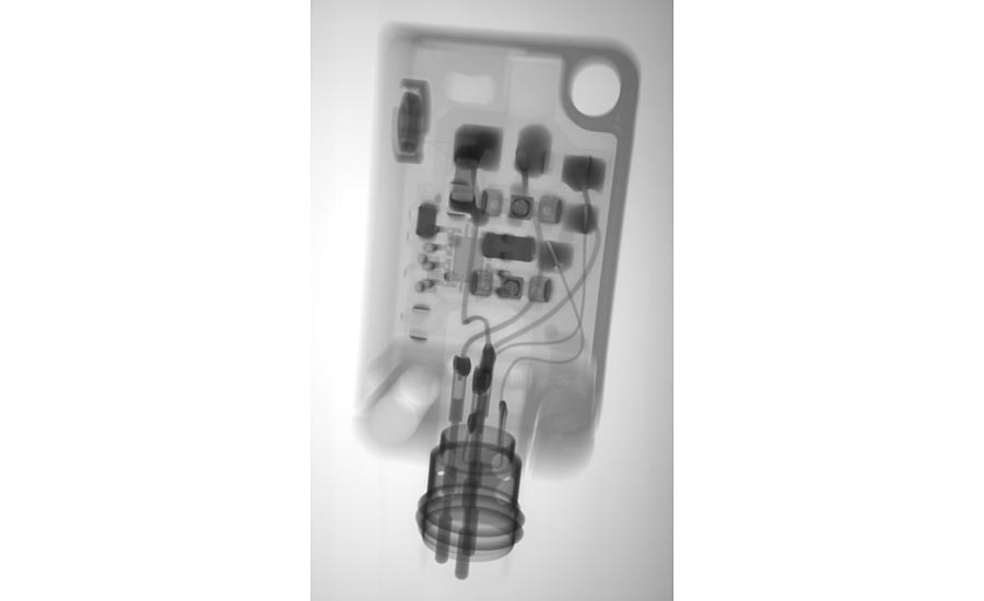
Figure 10. DR of a proximity sensor. Source: North Star Imaging Inc.
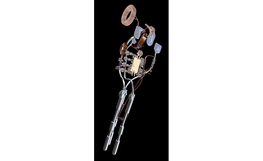
Figure 11. CT of a proximity sensor. Source: North Star Imaging Inc.
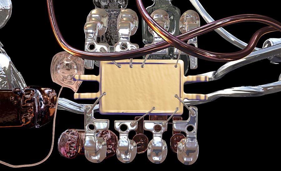
Figure 12. CT of a proximity sensor. Source: North Star Imaging Inc.
Another application of CT is in the area of metrology. Many product designs take on complex geometries with internal features and chambers that are not accessible for conventional measurements methods such as contact coordinate measurement machines (CMM). CT is now successfully solving this problem in many applications and is used to retrieve internal and external metrology data for product acceptance, while also providing data in monitoring build variability within a specific manufacturing process (See Figure 13). Automated software routines can be setup to provide multiple feature measurements while also performing automated routines for component placement of assemblies as well as product integrity evaluations such as porosity analysis.
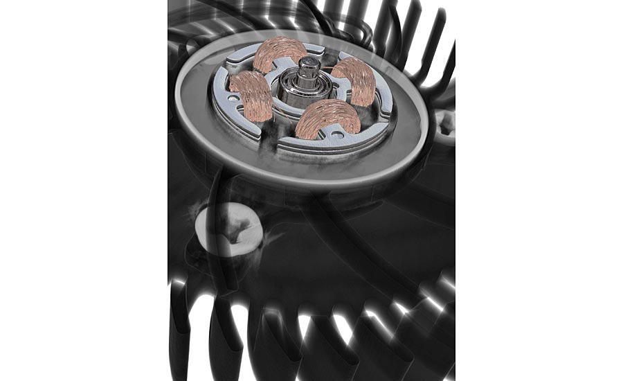
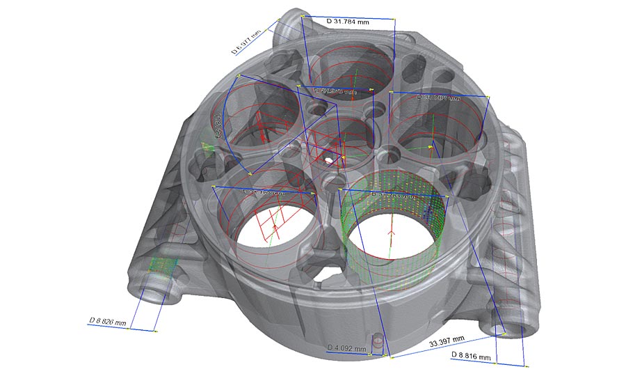
Figure 13. CT is now successfully solving this problem in many applications and is used to retrieve internal and external metrology data for product acceptance. Source: North Star Imaging Inc.
Summary
CT has expanded well beyond being used as only a research tool and is now being applied extensively in applications ranging from process and product development, process and product monitoring, sample through 100% inspection operations, product metrology and full-scale failure analysis and forensics work. Product samples vary in size from smaller than a human hair in diameter to many feet in length. System resolutions and applications can vary from the sub-micron range into the millimeter range. Today’s CT equipment is currently providing high quality CT scanning in a matter of seconds for some high-volume production applications. We have even performed 4D CT scanning of products by performing back-to-back CT scans of samples undergoing motion over time. An example would be of a gear turning within an assembly.
Recent innovations and advancements of CT technology and software developments have proven to further improve image quality while still reducing cycle times. These breakthroughs along with advanced techniques provide tremendous opportunities for companies to benefit from the use of CT in their day-to-day operations while assisting in accelerating the process of bringing new, high quality products to market.
*DR and CT images were produced by Matt Zachman and Brett Muehlhauser using NSI X-ray Systems
Looking for a reprint of this article?
From high-res PDFs to custom plaques, order your copy today!


