Vision & Sensors | Inspection
Exploring Integrated Optical Inspection Systems
For noncontact surface characterization of manufactured materials.

Source: LMI Technologies
Coordinate measurement machine (CMM)-based systems are often used for offline and at-line quality inspection. However, CMMs rely on robot arm movement and touch-probe data acquisition, which makes them slow and expensive systems.
As an alternative to CMMs, production engineers have the option of deploying versatile, noncontact optical inspection systems that allow for the implementation of first-article or random part inspection in a fast, nondestructive way and at roughly half the price of a CMM-type or other NIST-certified metrology system.
Noncontact Optical Inspection
Such systems provide noncontact surface characterization and reporting of multi-layered, textured, mixed, and a wide range of other manufactured materials. These systems are able to leverage different scanning technologies for maximum versatility, such as line confocal and laser profiler sensor technology to scan surfaces with submicron precision, and at a level of quality and speed that outperforms competing technologies.
Technology Advantages:
Integrated Line Confocal And Laser Line Profiler Sensor Technology
1. Integrated Line Confocal Imaging
3D line confocal sensors leverage a patented optical technique where white light emitting from a sensor’s transmitter is split into a continuous spectrum of wavelengths. The reflected wavelengths that are “in focus” return to the sensor’s optical receiver that maps wavelength variation to height or distance variation. The sensor’s off-axis design allows it to simultaneously carry out 3D topography, 2D intensity, and multi-layer 3D tomography scanning.
- Sub-micron Z precision
- Handles wide variety of material types
- Fast scan rates (max 16000 Hz)
- Simultaneous generation of multiple profiles on multi-layer structures
- Dual-axis arrangement enables multi-layer (tomography) scanning
3-in-1 Imaging Capability
When running 3D line confocal sensors, an optical inspection system can generate 3D topography (3D surface geometry), 3D tomography (multi-layer 3D geometry and 2D intensity), and 2D intensity data simultaneously.
Line confocal scanning avoids unwanted reflections from shiny metal surfaces and the off-axis arrangement is what permits multi-layer (tomography) scanning.
- 3D tomography scanning can be used to evaluate the physical properties of bonded glass elements
- 3D topography can be used for geometric dimensioning and surface and material layer defect detection
- 2D imaging can be used for simple object and defect detection
Multi-Layer 3D Profiling Capability
3D line confocal sensors contain embedded fast signal processing units, which detect all the surface layer 3D profiles in tomographic images. The height information of each measured data point can then be processed in calibrated micrometers. Finally, the intensity of every detected surface point is calculated at high resolutions.
Surface Defect Detection
3D line confocal sensors can be used in an optical inspection system for quality control of hybrid electronics and coated, transparent substrates to detect defects such as:
- Delaminations
- Scratches
- Impurities
- Air gaps
- Bubbles
2. Integrated 3D Laser Line Profiling
System support for integration with 3D line confocal sensors provides the production engineer with maximum scanning versatility. These high-speed sensors project a laser line onto the target, rapidly generating multiple profiles to form a high-resolution 3D image of the object, which can then be used for measurement, inspection, and metrology reporting.
Optical Inspection System Components
Noncontact optical inspection systems are composed of high-precision encoders, vibration-free movement, and automated stitching software to scan challenging materials–at large fields of view––in a variety of offline and at-line inspection and laboratory and R&D processes.
The system includes a vacuum table, industrial PC (with onboard motion path planning and standard inspection software), display, keyboard, mouse, joystick, and calibration block. Its surface characterization capabilities include part alignment, automatic feature detection and profile extraction, multi-coordinate measurement, Geometric Dimensioning and Tolerancing (GD&T), surface roughness analysis, and more.
1. Integrated Hardware Platform - High-precision and vibration-free motion system
- High resolution (0.4µm) encoders for X, Y, Z axis
- High-performance servo driver
- Vibration-free marble table
- Multi-coordinate controls allow for easy part positioning and programming
2. Integrated Software Platform
- All-in-one software platform has a user interface that makes inspection fast, easy, and flexible
- Offers a multitude of feature detection and construction tools that enable automatic extraction of part geometry
- Generates a metrology report (see Fig.1) for surface characterization analysis
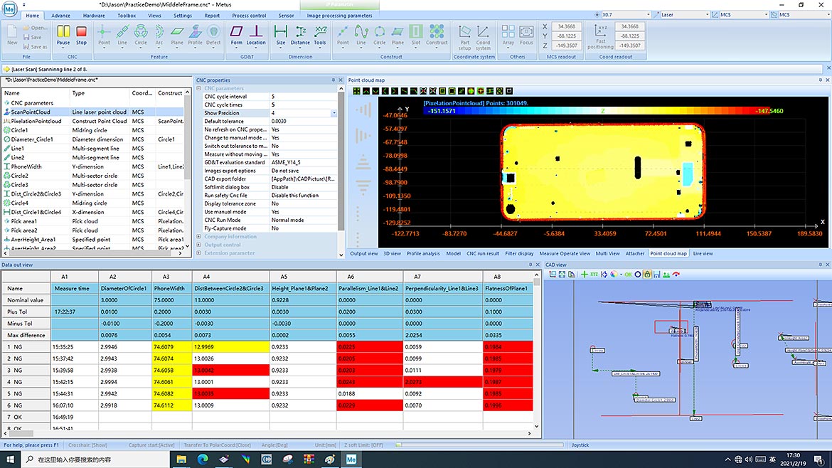
Figure 1 | Source: LMI Technologies
Surface Characterization Applications With Smart 3D Line Confocal Imaging (LCI)
Surface Roughness
In many manufacturing applications it is necessary to systematically inspect surface roughness in order to ensure tight manufacturing tolerances are met. A noncontact optical inspection system leveraging LCI technology delivers nondestructive, ultra-fast scanning and analysis of surface microtopography with real-time reporting for a range of automated production processes.
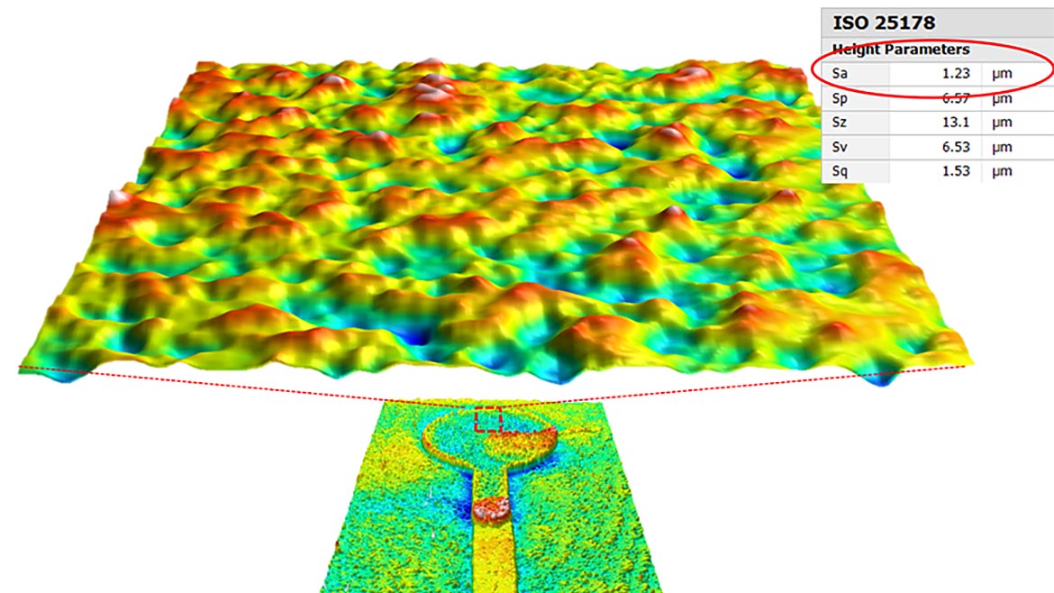
Surface roughness of silver epoxy pad | Source: LMI Technologies
Multi-Layered Cell Phone Display Glass
The combination of 3D tomography (multi-layer) and 2D intensity imaging is used to identify defects such as delamination, scratches, or dust on the surface of laminated glass, mobile phone displays, or any other type of transparent multilayered material like sealed medical packages.
And, contrary to other types of imaging systems, line confocal sensors detect not only the location of the defect, they also identify in which layer the defect exists. The sensor even measures the dimensions of the defect down to the sub-micron level.

Multi-layer cell phone display glass inspection with LCI | Source: LMI Technologies
PCB-to-Chip Solder Ball
There are thousands of tiny solder balls on the PCB board for connecting the chip and the PCB. In the past, it would take significantly more time to measure these solder balls with a microscope. With noncontact optical inspection, you can complete the measurement of all solder balls in just minutes. Measurements include ball height, spacing and X/Y position, and defects (e.g. shape or missing material on the topmost region of the solder ball).
UV Protective Glue Surface
UV protective glue adhesive strengthens the bonding of ICs (integrated circuits) and FPC (flexible printed circuit) substrates and makes the assembly waterproof, dustproof, and protects against salt spray. Usually the UV protective glue is transparent, which makes it difficult for other optical metrology systems to inspect the dimensions or defects of the glue.
With noncontact optical inspection leveraging LCI, you can accurately measure and inspect the 3D glue height and volume before it is cured, which prevents the occurrence of excess adhesive volume or broken glue beads.
Medical Seal
LCI-based noncontact optical inspection provides a powerful method for automated medical seal verification. This technology develops high resolution 3D and 2D scan data of the internal structure of the blister pack layers and pouches commonly used in medical packaging. With multi-layer data acquired from inline scans of the sealing regions, defect detection software can isolate contamination and air gaps, flag incomplete sealing, and detect defects such as wrinkles and burn marks.
- Automated inspection of pharmaceutical and medical packages
- High resolution 3D images of transparent seal layers
- Fast, noncontact, nondestructive optical verification
- Detects internal seal defects invisible to the human eye
- User programmable to handle different material types
Semiconductor
LCI-based optical inspection delivers precision 3D scanning and inspection at various stages of the semiconductor fabrication process for maximum product quality and optimal production throughput.
- Wafer sorting
- Wafer dimensional characterization and defect detection after scribing
- Characterization of BGA and PGA position, height, and radius during assembly and test IC
- Characterization of silver epoxy during die application
- Defect detection in wire bonding process
- Dimensional characterization during ball-bumping process and final packaging
- Multi-substrate defect inspection and metrology
- Advanced surface inspection of compound semiconductor materials
- Defect inspection on SiC and GaN substrates
- Hard disk drive media and substrates defect inspection, topography measurement, and classification
- High throughput defect inspection for large and irregular shaped substrates
- Unpatterned wafer flatness measurement
- Wafer warp/bow inspection
- Wafer edge roll-off inspection
- Wafer edge geometry measurement and defect detection
- Sub-micron (i.e. deep) surface defect detection
- Global and local wafer topography measurement
Battery Weld Seam
With a noncontact optical inspection system you can quickly measure dimensions (e.g. correct height and volume) as well as identify defects in the battery weld seam including breakages, overflow, offset, cracks, air holes, excessive roughness, discoloration, and more.
Why Choose Noncontact Optical Inspection?
Metrology Reporting
Production engineers need to generate a “report card” of parts (first-article or random) they have pulled off the production line in order to measure relative differences in shape from part to part or compared to a “golden” master part. The software that comes with a product is able to generate a metrology report with the same requirements as those generated from competing technologies.
Specialized Measurement Capabilities
Leveraging a patented line confocal sensor technology, an LCI-based platform is capable of delivering high-precision 2D/3D surface characterization of multi-layered, transparent/translucent, and curved-edge materials.
Automated 3D Image Stitching
Noncontact optical inspection provides the ability to automatically stitch multiple 3D images means you can achieve multi-sensor results with a single sensor. This saves you the time, effort, and cost of having to acquire, setup, synchronize, and manage multiple sensors on your own. The motion system is even able to stitch 3D images in the X, Y, and Z directions.
Also Suitable for R&D Projects
In addition to QC applications, noncontact optical inspection can also be used by lab and R&D engineers for rapid GD&T surface characterization in prototype evaluation, or to verify supplier specifications (e.g. on an internal component that is integrated into a larger assembly).
Looking for a reprint of this article?
From high-res PDFs to custom plaques, order your copy today!


