Vision & Sensors | Camera Interfaces
CLHS IP Core Enables 25 Gbps Products To Quickly Reach The Market
CLHS uses a proven core that is easy to use, operates at 10g, 25g, and has a roadmap to 50g.
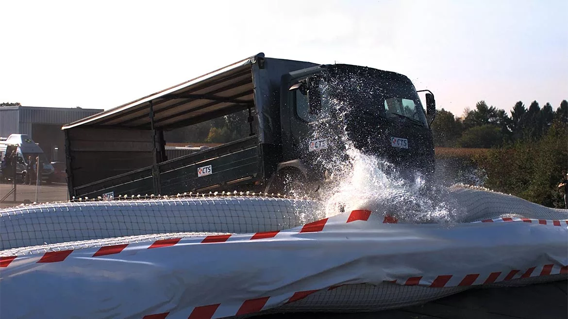
Crash test applications can benefit from the 25 G optical fiber interface of Camera Link HS (CLHS). Image is captured by an Excelitas PCO camera. | Image courtesy of Excelitas PCO GmbH
The CLHS X protocol 25 Gbps IP Core is the same IP core that is found in all the 10 Gbps CLHS products on the market and has been available from the A3 since the original release of the CLHS specification in 2012. This proven core presents easy-to-use parallel interfaces for video, bidirectional trigger, camera commands, bidirectional GPIO, and the CLHS revision message. Performing all the priority encoding requirements listed in the CLHS specification, the core simplifies developing CLHS products. The associated PCS module does 64/66b encoding with forward error correction ensuring error-free transmissions and enabling the core to be used with FPGA transceivers that offer simple 64-to-1 serializers/deserializers. No other IP is needed.
CLHS specification 1.2 recently introduced the 25 Gbps speed along with the QSFP28, SFP28, and MPO connectors. The good news is that 25 Gbps optical engines are backward compatible to 10 Gbps optical engines where CLHS discovery occurs. CLHS uses a failsafe negotiating process to switch to 25 Gbps. Several developers have already developed 25 Gbps systems using proven 10 Gbps hardware to debug the 25 Gbps product. The committee has proof of concept to achieve 50 Gbps using the same IP core, ensuring an easy transition to future speeds.
This paper describes the steps to create a CLHS 25 Gbps solution in an FPGA for a camera containing a monochrome image sensor having 2048H x 1024V pixels with 12-bit output running at 950 frames a second. It is desired to send this 2.99 GByte/sec data to the host for processing; 2.99 GByte/sec is within the 3 GByte/s capability of a single CLHS lane at 25 G. An SFP28 solution is chosen.
The open VHDL core purchased from the A3 for $1000 (Camera Link HS Standard: The High-Speed Interface for the Future of Imaging and Machine Vision (automate.org)) includes the CLHS camera and frame grabber modules and the CLHS PCS making a complete system as shown below.
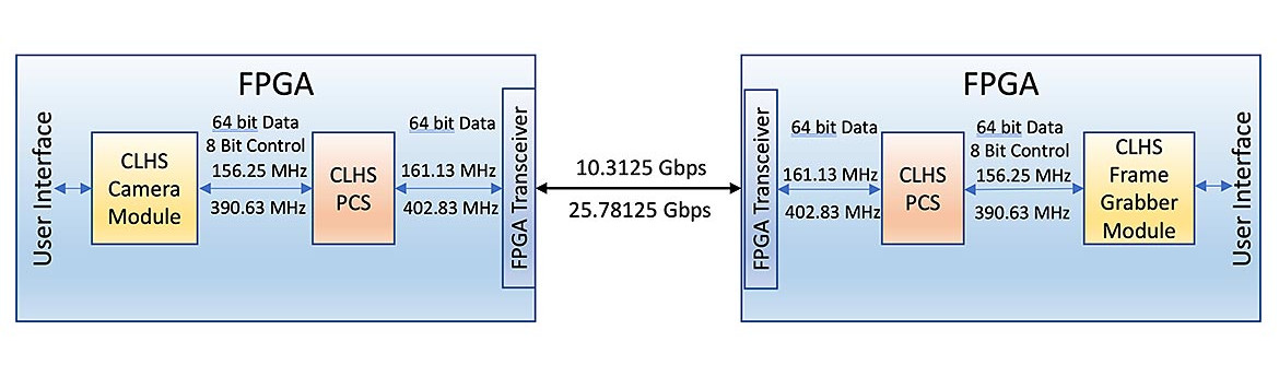
Image Source: Teledyne DALSA
The core is not specific to any vendor and has been implemented on AMD (Xilinx), Intel (Altera), and MicroChip (PolarFire) FPGAs. The developer needs to configure the transceiver function, the clock distribution, and the logic that feeds/gets messages to/from the core. The figure below shows the IP core’s virtual message channels of Pulse (trigger), GPIO, Video Data, Command, and Revision. The transceiver configuration and clock distribution are configured by the users of the core. All the packet building, encoding, and priority rules are handled by the CLHS core. During discovery, the frame grabber reads the mandatory registers in the camera and decides to initiate the transfer to 25 Gbps operation, which requires the transceivers to be reconfigured and any associated PLLs to be reset.
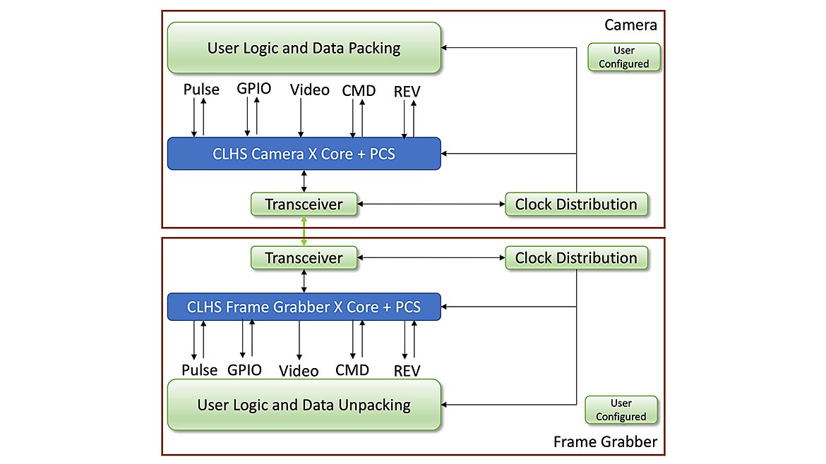
Image Source: Teledyne DALSA
Using The Core
Vision & Sensors
A Quality Special Section
The core presents easy-to-use parallel interfaces. As an example, the pulse message is sent by setting the desired pulse mode and the associated bytes in the parallel interface, and then a one-clock-wide pulse is applied to the send request input pin. The Pulse message is then transmitted over the link, where the CLHS receiver decodes the message type, and signals the parallel data availability to the user’s system with a one-clock-wide PulseMsgValidStrobe pulse. GPIO and Revision messages use identical methodologies. The video and command packets can be up to 8k and 1k bytes respectively in size. The user writes the 64-bit or 32-bit data respectively into the CLHS buffer with a write enable pulse and when finished writing the packet data, and setting the parallel header byte content, issues a one-clock-wide send request on the message port which causes the IP core to send the message onto the link. At the receiver the incoming packet is decoded and correctly stored in the video or command receive buffer and asserts a one-clock-wide pulse, such as VidMsgValidStrobe, to signal that the buffer is ready to be read.
Let’s consider the video message as an example for setting the header information. CLHS is a remote DMA-style packet using RowID and ColumID to define the pixel location of the first pixel in the packet. The sensor under consideration is 2k pixels wide and the 12-bit data is concatenated, resulting in 3kbytes for a single row of data. This easily fits in the 8k byte maximum. If the data rate of the sensor was faster, then one could add a second lane and send even row data on lane 0 and odd row data on lane 1 or choose to send pixel 0 to 1023 on lane 0 and pixel 1024 to 2047 on lane 1. The choice is up to the user and how the user chooses to fill the CLHS data buffers. With this example, only one lane is needed, and the first pixel of each row is column 0. By convention, the first row of a frame is row 0 and is incremented for each row output from the camera. If the sensor is top/bottom readout then row 0 is the first row of the frame and row 1023 is the second row from the camera, setting row ID to 0 then 1023 as input to the CLHS core. CLHS is a data push model, so cameras do not need to buffer image data. The developer decides to support older frame grabbers with 10G capability and designs in 2 fiber connections, achieving 2.8 GByte/sec of bandwidth and the ability to configure the camera to use a single 25 G lane for full frame rate. The configurations that the developer decides to support in the camera are listed below and documented in the mandatory CLHS registers so that the frame grabber can auto-negotiate the setup.
The values applied to the CLHS camera Video IP core are shown in the table below. The small v prefix in the port names indicates that the clock used for this interface is a customer-supplied video clock and all signals are synchronous to this clock. The frame grabber core has corresponding signals except where the inverse function is needed such as vRdEn input and vVidDataAvailable, vVidMsgValidStrb, and vVidDataValid.
Conclusion
CLHS uses a proven core that is easy to use, operates at 10G, 25G, and has a roadmap to 50G. Products can be developed at 10G using proven partner products and when debugged can make the move to 25 G. For customers that don’t need the speed of 25 G, they can use 10 G optical engines which are lower cost and power connecting to 10G frame grabbers which are anticipated to be lower cost than higher performing 25G products.
Looking for a reprint of this article?
From high-res PDFs to custom plaques, order your copy today!


