With XRF Measurement, the Goal is Achieving Low Limits of Detection Precisely—and Fast
Here’s how to get there.
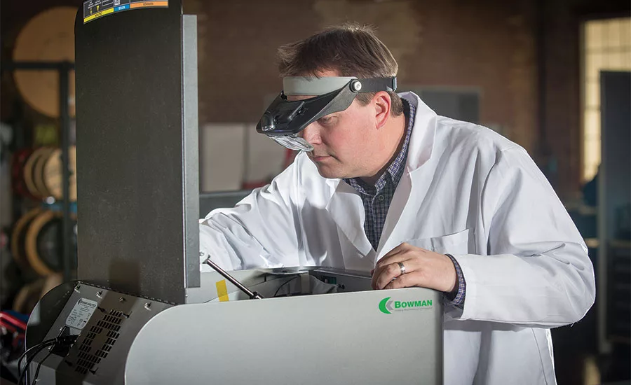
XRF coating thickness measurement instrument with silicon drift detector. Periodic inspection of the measurement head is one of the few maintenance tasks needed for this system. Source: Bowman
X-ray fluorescence is an elemental analysis tool that has been a mainstay of test labs for decades. A versatile NDT method that demands only minimal sample prep and can be run by novice operators, it is perhaps most valued for delivering accurate results quickly. Today, evolving XRF capabilities are moving this quality assurance workhorse into critical new roles in a widening spectrum of industries.
XRF is based on the concept that individual atoms, when excited by an external energy source, emit X-ray photons of a specific wavelength. By counting the photons of each energy emitted from a sample, the sample’s different elements can be identified.
In manufacturing, virtually every metal product is coated (usually electroplated) or treated (anodized or galvanized) to enhance anesthetics, or improve performance properties. XRF is the leading technology worldwide for the measurement and quantification of these finishes. XRF is applicable to the testing of any metallic coating, single or multi-layered, over any metallic or non-metallic substrate.
In tech, PCBs, wafers, semiconductors and their components all have “final finishes” that are central to their functionality. Here as well, XRF measurement is the standard technique for determining what does—and does not—meet specifications.
Coating thickness measurement is the most common, and most-discussed function of XRF in industry, but it is not its only purpose. Quality XRF systems also perform alloy analysis, and solutions analysis. XRF can determine the percentage composition for each alloying element and identify the alloy grade number. For solutions analysis, metal ions in plating baths can be quantified for process control.
Wherever XRF is used, its two “opposing ends”—emission, where the X-ray is generated, and detection, where the signal is processed—determine what a specific instrument can achieve, how precisely (and cleanly), and how fast.
The Emission Side
Entry level XRF systems use pin hole collimators, which filter the X-rays so that only those traveling parallel to a specified trajectory can pass through. The size of the collimator determines the size of the irradiation spot projected onto the sample. XRF instruments have single or multiple collimators depending on the geometry and the size range of the parts being tested.
The alternative to collimation is polycapillary optics. This is X-ray enhancement at its finest, created to compensate for the fact that the X-ray source cannot, on its own, generate a high density beam. Polycapillary optics uses focusing components as opposed to pin holing the X-ray beam to its target.
It was initially employed as a research tool by national labs and others involved with small feature analysis and elemental mapping, but when industry saw its potential for process and quality control, instrument companies re-thought the technology, adding features, enhancing image resolution, and boosting measurement speeds.
Faster speeds—a particular priority for industry—are enabled by a smaller X-ray beam, and a flux that’s 100X higher than a collimator. The higher flux allows the counting of more photons, and greatly enhances the precision of the analysis.
Polycapillary X-ray optics is comprised of hundreds of thousands of stand-alone glass channels that collect a large solid angle of X-rays emitted from a diverging source. The X-rays pass through the optic by total external reflection and are focused to an extremely small spot with ultra-high intensity. These optics also deliver a very clean excitation beam, compared with one from a collimator, because there’s no scatter from the pinhole, and the focal spot is extremely well defined.
Although it sounds fragile, a polycapillary optics assembly is extremely robust. Users report that the only issue is if someone crashes a sample into it. Customers buy it, and have it for a lifetime.
Because the applications that benefit from polycapillary optics are those with very small features, this option has tracked perfectly with the miniaturization that defines electronics manufacturing. The most elite systems can focus X-ray excitation down to sample regions as small as 7µm.
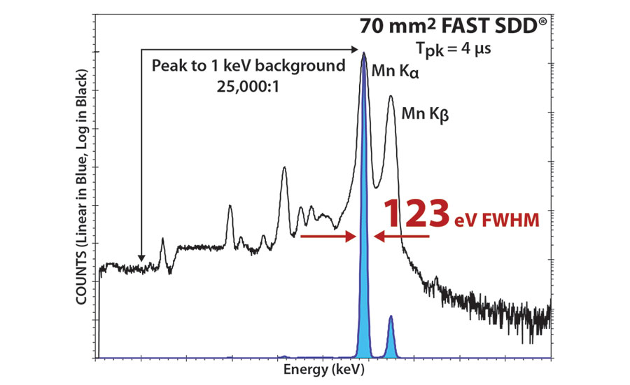
Silicon drift detector spectrum shows a highly favorable peak-to-background ratio with suppressed noise and higher resolution.
The Detector Side
XRF instruments used for coating measurement use one of three types of detectors: a “Prop” (Proportional) Counter, a Silicon PIN Diode or a Silicon Drift Detector (SDD).
Proportional counters are gaseous ionization devices that measure the energy of incident radiation by producing a detector output proportional to the radiation energy.
Prop counters have a generous detector window for capturing the fluoresced X-rays. They operate in an intermediate voltage range and are well suited to the measurement of conventional single-layer (and some multi-layer) electroplated deposits.
Proportional count instruments are lowest in price of the three, and ideal for simple applications where there’s no need for high resolution to see the separation of peaks on the spectrum. Their downsides include high baseline noise, and the need for frequent calibration.
Temperature control for these devices is critical, because the detector uses a gas that’s highly sensitive to temperature change—much more than any solid state detector. The gas-filled tube also has a tendency to leak over time. Despite its disadvantages, it has a generally higher flux due to the large window, so it detects a high number of photons. The applications may be limited, but the standard deviation is better.
The silicon PIN diode provides spectral resolution superior to that of a proportional counter. This means operators can measure thinner deposits and lower element concentrations, and perform more complex measurements such as those on alloys and heavily layered samples and those involving unidentified materials. Silicon PIN detectors are low noise, have excellent resolution, excellent detection limits and are extremely stable, thanks to Peltier (TEC/TEM) cooling.
Silicon drift detectors produce the highest count rates, and the highest spectral resolution—typically 50% higher than silicon PIN diode detectors. They offer significant peak to background ratio improvement compared with prop counters. They have the lowest baseline noise, the best detection limits and the greatest versatility in terms of element testing range.
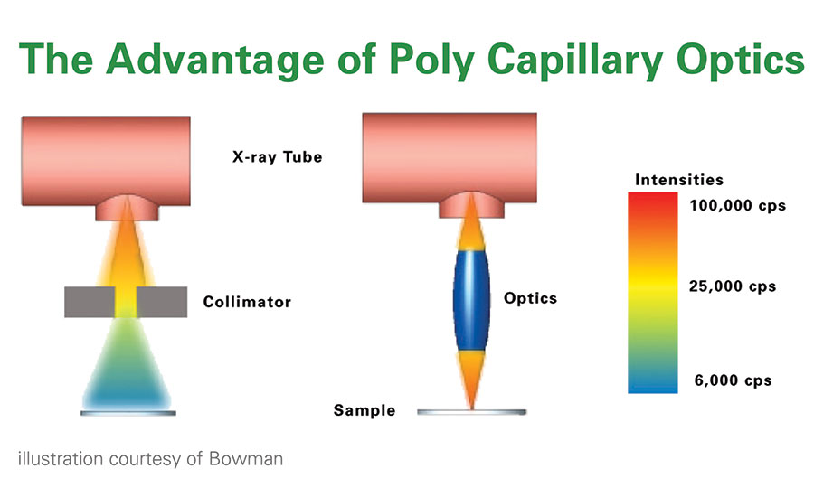
Polycapillary optics substantially accelerates photon counting for XRF measurement devices. Source: Bowman
Because they are most effective at eliminating background noise, SDDs are best able to precisely measure the overlapping elements—those “neighbors” on the periodic table, nickel, copper, zinc and chrome and iron—where the separation of signals between them is minimal. With old technology, there was no way to resolve these overlapping elements without mathematical calculations. Today, the improved resolution provided by both silicon PINs and silicon drift detectors eliminates the need for mathematical calculations or numerical filtering.
Also like Silicon PINs, silicon drift detector chip sets are Peltier cooled, free from climate effects and nitrogen reservoirs. There is virtually no maintenance required for these detectors. SDDs are the detector of choice for films below 50 µm, and complex films used in the technology sector, including ENIG, EPIG and ENEPIG (Electroless Nickel Immersion Gold; Electroless Palladium, Immersion Gold, and Electroless Nickel Electroless Palladium, Immersion Gold, respectively).
Notably, silicon PIN and silicon drift detectors, the two solid state options, are recommended by new IPC (industry association for printed circuit board and electronics manufacturing manufacturers, their customers and suppliers) standards, 4552 and 4556. These are broadly applicable to specialty coatings used throughout the PCB and the wider electronics sectors.
Looking for a reprint of this article?
From high-res PDFs to custom plaques, order your copy today!


