Machine Vision
Line-Scan Imaging and Illumination in Modern Machine Vision
Sensors, illumination, 3D, and the role of AI in high-throughput inspection
Line scan camera captures accurate images of cosmetic defects on transparent surfaces at frequencies topping out at a maximum speed of 47.72 kHz at 850 megapixels per second.
High-throughput manufacturing inspection presents constraints that don’t yield to general-purpose solutions. Continuous webs move hundreds of meters per minute. Semiconductor wafers pass through process tools without pausing for measurement. Food products on conveyor lines present organically variable surfaces requiring simultaneous evaluation for contamination, dimensional conformance, and fill level. These environments share one requirement: the imaging system must acquire spatially uniform, consistent data at speeds and scan widths that expose the fundamental design limitations of area-scan cameras.
Line-Scan vs. Area-Scan
An area-scan camera integrates light across a 2D pixel array and reads the entire matrix in a single frame. Area-scan sensors expose all pixels simultaneously (global shutter) or near-simultaneously (rolling shutter) and then read out the frame. At high conveyor speeds, the integration time required to accumulate sufficient signal introduces motion blur proportional to velocity — a constraint that can only be mitigated by sacrificing sensitivity, increasing illumination, or using strobed lighting powerful enough to freeze motion within the exposure window.
A line-scan sensor replaces the 2D array with a single row of photodetectors. Each line is exposed and read in microseconds, with successive lines assembled into a composite image as the target moves. Because integration time per line is short and consistent, motion blur is determined by line rate and conveyor speed — a relationship the system designer directly controls. The resulting image can be of arbitrary length, bounded only by the extent of the target, and can achieve spatial uniformity across large fields of view that is challenging to maintain with area-scan systems.
Critically, line-scan cameras decouple lateral and longitudinal resolution. Pixel count along the line — ranging today from 2k to 32k and beyond through multi-row synthetic resolution techniques — defines cross-web spatial resolution independently of acquisition speed. Line rate defines along-web resolution independently of pixel count. Multi-row CMOS sensors with staggered pixel offsets can generate synthetic resolution substantially higher than the physical pixel pitch suggests, enabling sub-pixel-scale defect detection on semiconductor and PCB surfaces. Modern CoaXPress-12 interfaces support these data rates, with monochrome line rates exceeding 240 kHz now commercially available.
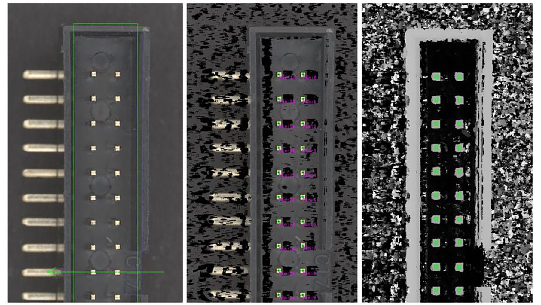
Line-scan system uses an algorithm to detect the number of pins and creates corresponding regions of interest within a grid to calculate the 3D position of every pin relative to others while measuring pin width (radius) and length. Source: Allied Vision
CCD vs. CMOS Line-scan Sensors
CCD line-scan sensors offer low read noise, high charge-transfer efficiency, and well-characterized spectral response. Trilinear CCD configurations — three parallel rows filtered for R, G, and B — provide true color registration at the pixel level, making trilinear CCD a long-favored architecture for color-critical applications such as print inspection, pharmaceutical label verification, and textile grading where color measurement accuracy matters.
CMOS line-scan sensors offer higher peak line rates, lower power consumption, and greater readout flexibility. Contemporary CMOS designs can simultaneously acquire RGB plus near-infrared across the 400–960 nm range in a single pass. For applications where surface chemistry and appearance must be assessed concurrently — battery electrode inspection, where NIR penetration reveals subsurface coating uniformity, or food quality grading, where NIR distinguishes water content from surface color — simultaneous multispectral acquisition eliminates the registration challenges of sequential channel switching.
Spectral coverage now extends well beyond the visible range. SWIR sensors (900–1,700 nm) reveal moisture distribution in food, subsurface delamination in composite materials, and contamination hidden beneath surface coatings. UV-sensitive configurations detect fluorescent markers and surface chemistry signatures relevant to pharmaceutical and electronics inspection. Selecting the appropriate spectral range is as fundamental a design decision as selecting spatial resolution.
Stable, Flicker-free LED Illumination
Of all parameters in a line-scan system, illumination most consistently determines whether theoretical sensor performance is realizable in practice. A line-scan camera acquires exactly one row of pixels per exposure — there is no inherent spatial averaging across multiple lines, and no opportunity to compensate for illumination non-uniformity during image formation. A brightness gradient of only two or three percent across the illumination line appears directly in the image as a systematic artifact, indistinguishable from a real surface feature until calibrated out.
Legacy light sources — fluorescent, halogen, and metal-halide — cannot be practically strobed at line rates in the tens to hundreds of kilohertz range. Their spectral output shifts with temperature and age, introducing drift that recalibration cannot fully track. High-intensity LED illuminators engineered for line-scan applications address each of these limitations: electronic modulation at line rates is native to LED drivers, spectral output remains stable over operational lifetime, and precision optical design concentrates flux into the illumination line with controlled homogeneity.
The geometric configuration of illumination relative to the surface is as important as intensity. Dark-field illumination at a grazing angle emphasizes surface topography — scratches, embossing, and texture — by exploiting the differential scattering of oblique light. Bright-field illumination emphasizes reflectance and color. Multi-field configurations, enabled by modern LED controllers with independent channel timing, can sequence through multiple illumination geometries within a single inspection station, presenting the downstream pipeline with a multidimensional dataset from a single physical pass.
Spectral choice in illumination is a design variable, not a default. Monochromatic illumination matched to the target’s optical response — red light on red-filtered substrates, blue light on copper or organic dyes, and UV illumination to stimulate fluorescence — can substantially increase defect contrast and reduce the burden on downstream image processing.
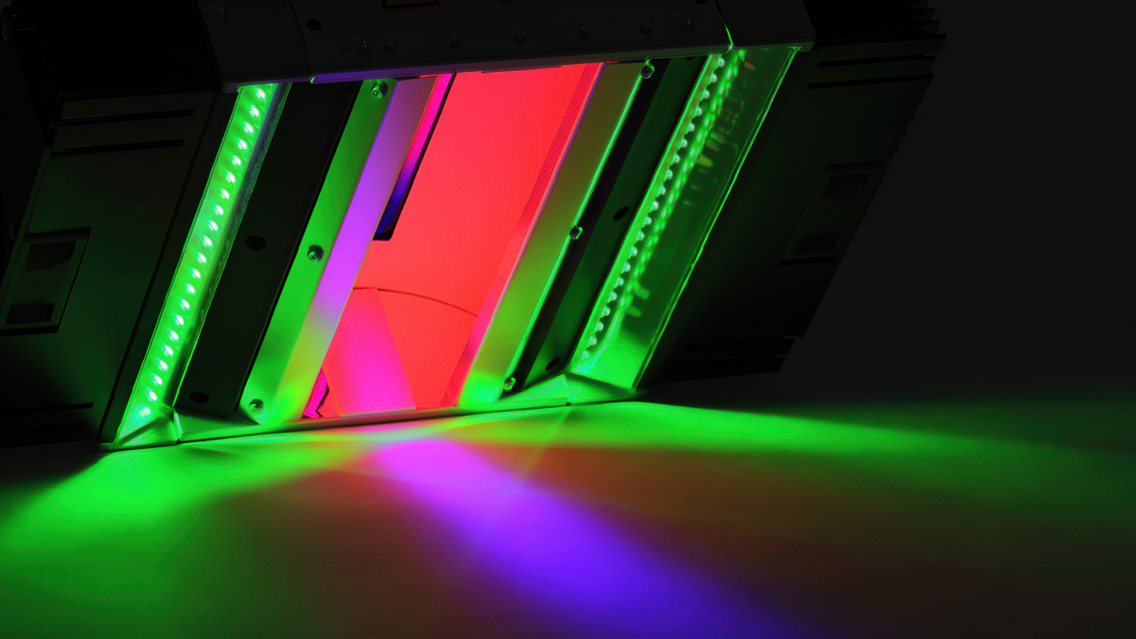
Illumination intensity is mission-critical in 3D line-scan applications. As line rates climb for high-speed capture, shrinking exposure windows demand proportionally greater light output. Source: Allied Vision
3D Line-Scan at Production Speeds
A growing class of inspection problems requires height data that 2D imaging cannot provide: solder joint height, substrate bow, fill level, and dimensional conformance of formed metal components. Stereo photogrammetry has emerged as a commercially mature approach that can preserve high line-scan throughput while adding simultaneous 2D color acquisition.
In a stereo line-scan system, two cameras at a fixed baseline angle image the same line on the target surface. GPU-accelerated stereo disparity algorithms compute pixel offsets between corresponding features in the two images and convert that disparity to height via calibrated geometry, generating a dense 3D point cloud for every line in real time. The 2D color image is acquired simultaneously and co-registered with the 3D data, without a secondary pass.
Performance spans a wide operational range. At the high-resolution end, optical resolutions on the order of 2 µm with sub-micron height resolution over ~16 mm fields suit semiconductor failure analysis and flip-chip assembly verification. At intermediate resolutions, 6–7 µm optical resolution over 100 mm fields covers PCB solder inspection and precision machined component tolerancing. At the wide-field end, ~200 µm resolution over 1,400 mm fields addresses automotive body panels, ceramic tile, and wide-format food conveyor lines.
Laser triangulation, which projects a structured light line and measures its geometric distortion from a laterally offset camera, remains dominant for surface profiling applications requiring height-only measurement. Where simultaneous 2D and 3D data are required in a single pass, stereo line-scan provides a more integrated solution.
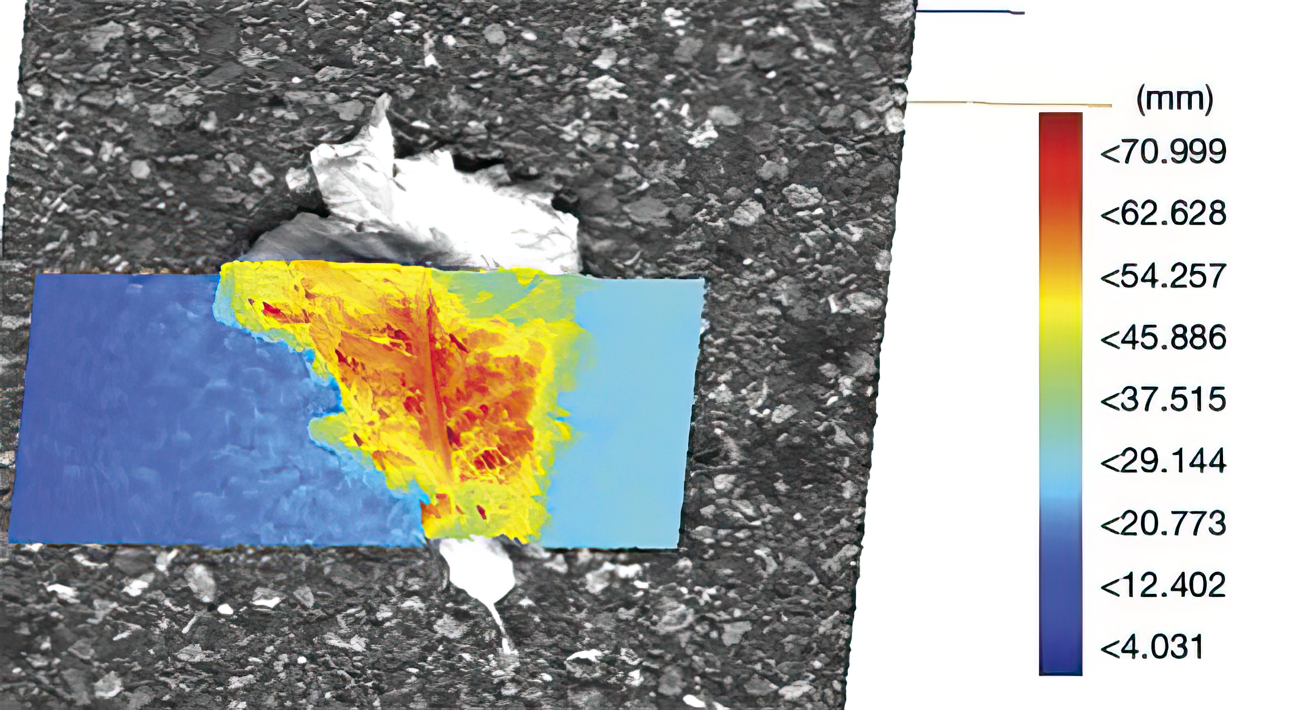
Line-scan 3D cameras can feature depth-sensing technology to detect road defects like potholes in real time, straight from a moving vehicle. Source: Allied Vision
AI in Line-Scan Inspection
The integration of deep learning into production inspection pipelines has changed the requirements placed on imaging hardware. Rule-based machine vision algorithms are relatively tolerant of systematic imaging artifacts because the algorithm designer can account for known non-uniformities during rule formulation. A trained neural network is typically less tolerant: it learns from the statistics of the training data, and systematic artifacts — illumination gradients, spectral drift, and line-to-line gain variation — can be learned as features of the image distribution. When the production imaging system drifts from training conditions, defect-detection performance degrades in ways that are difficult to diagnose.
This dynamic places a premium on exactly the characteristics that well-designed line-scan systems provide: spatial uniformity, radiometric consistency over time, calibrated spectral response, and high signal-to-noise ratio. Training data acquired on a stable, well-calibrated system produces models that generalize reliably to production conditions.
Multimodal training data — simultaneous 2D surface appearance and 3D height from a stereo line-scan system — enables classifiers that substantially outperform single-modality models where surface appearance and geometry are jointly discriminating. Cold solder joints and bridged joints may be difficult to distinguish by 2D color alone but are unambiguous in 3D data because their height profiles are geometrically distinct.
The trend toward edge-deployed inference is well matched to high line-scan data rates. A 32k monochrome camera running at 100 kHz generates over 3 GB/s of raw pixel data. Modern CoaXPress-12 interfaces combined with embedded FPGA preprocessing and GPU inference nodes make edge-deployed AI inspection at full line-scan resolution architecturally feasible in systems that would have required centralized server infrastructure until recently.

In flexo, gravure, offset, and digital presses, the substrate moves continuously. A line-scan camera captures one thin line of pixels at a time and builds the full image as the web moves. Source: Allied Vision
System Integration Considerations
Encoder synchronization is foundational. A mismatch between encoder pulses per line and actual surface velocity produces geometric distortion — compression or stretching along the conveyor axis — that cannot be corrected without knowing the true velocity. Telecentric lenses are preferred for dimensional measurement applications because they eliminate perspective-induced size variation at the edges of deep fields. Interface selection — CoaXPress-12 has largely displaced Camera Link for new high-resolution designs — affects data throughput, cable length, latency, and the processing hardware ecosystem. Software library compatibility with HALCON, MIL, or AI-focused toolkits should be evaluated before hardware selection is finalized.
Line-scan imaging’s position in machine vision is not fundamentally threatened by increasing area-scan sensor capability. Its architectural advantages for continuous, high-throughput, large-format inspection are structural — they derive from acquisition geometry, not sensor performance metrics that area-scan cameras could match in principle. What has changed is the sophistication of what can be done with line-scan data: 3D point clouds generated in real time, simultaneous multispectral datasets, and neural-network classifiers extracting defect intelligence from data streams that rule-based systems could never fully exploit. The imaging system has become the upstream constraint on how much intelligence can be extracted downstream.
AUTHOR NOTE: This article was contributed by Chromasens, which is now part of a broader Allied Vision brand. In January 2026, the machine vision brands Allied Vision, Chromasens, Mikrotron, NET, and SVS-Vistek were united. This strategic step enables customers to move more quickly from consultation to implementation with integrated cameras, frame grabbers, software, accessories, and application support from a single source. Learn more at www.alliedvision.com.
Looking for a reprint of this article?
From high-res PDFs to custom plaques, order your copy today!


