Management
Building Quality Systems for Semiconductor Yield Ramp and High-Volume Production
In this Q&A, Anshul Karnik discusses how manufacturers build quality systems capable of supporting new-product introduction, yield ramp, and high-volume production in increasingly complex semiconductor environments. He explains how process capability, adaptive sampling, virtual metrology, and statistical process control help organizations identify risk earlier, accelerate learning, and maintain manufacturing readiness as production scales.

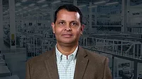
Anshul Karnik is a manufacturing and quality leader whose work focuses on one of the semiconductor industry’s most challenging transitions: moving advanced technologies from development into stable, high-volume production. Across roles spanning foundries, semiconductor equipment suppliers, and large-scale manufacturing environments, he has concentrated on the quality systems, process-control frameworks, and metrology strategies that determine whether a technology successfully scales while maintaining yield, reliability, and operational consistency.
Anshul’s experience covers the full lifecycle of semiconductor manufacturing, from sub-10-nanometer process development and advanced metrology to yield stabilization and ramp readiness under high-volume production constraints. In these environments, manufacturing success is defined not by isolated technical breakthroughs, but by the ability to manage variability, risk, and learning speed as complexity increases.
A defining feature of Karnik’s work is his emphasis on designing manufacturing as a responsive system. By applying statistical process control, adaptive sampling strategies, and machine-learning–driven virtual metrology, he has helped teams identify instability earlier, allocate metrology resources more effectively, and accelerate transitions into volume production without compromising reliability.
In this interview, Karnik discusses the technical and organizational challenges of semiconductor NPI, how yield ramp exposes hidden manufacturing risks, and what it takes to move emerging technologies into high-volume manufacturing with confidence.
ELLEN WARREN: You’ve spent much of your career operating at the boundary between technology development (TD) and manufacturing execution. What makes the transition from TD and early NPI into yield ramp and HVM uniquely difficult in semiconductor environments?
ANSHUL KARNIK: The transition is exceptionally difficult because the ramp environment is fundamentally unstable and highly sensitive to atomic-scale tolerances where even minor process variations can collapse yield. Unlike mature nodes with predictable system noise, early production faces unpredictable shifts driven by immature process windows, chamber matching issues, and unrefined processes. Managing this instability requires a shift from manual parameter tuning and offline metrology to highly responsive, data-driven production disciplines.
EW: Yield ramp is often described as a manufacturing problem, but in practice it behaves more like a systems problem. In your experience, what failure modes tend to surface during ramp that are rarely visible during early development?
AK: During early development, engineers often optimize for a single golden tool, but yield ramp quickly exposes systems-level issues like tool matching variances and chamber instabilities across the broader fleet. Also, latent reliability defects such as electromigration or time-dependent dielectric breakdown (TDDB) often only emerge when scaling up volume, posing massive warranty risks. These unpredictable shifts demand continuous, real-time oversight rather than relying on the isolated technical successes achieved in R&D.
EW: As process complexity increases, metrology capacity itself can become a constraint. How do you think about metrology strategy when scaling from pilot production to high-volume manufacturing?
AK: Metrology strategy must evolve from heavy, static physical inspection, which creates severe cycle-time bottlenecks and consumes valuable cleanroom resources to dynamic, risk-based frameworks. I believe in an AI-enabled Adaptive Process Control (APC) strategy that scales metrology based on real-time process capability (Cpk). If a process is stable, we minimize physical measurement and rely on virtual metrology; if it drifts, we immediately increase sampling to protect yield.
EW: You’ve been a strong proponent of Cpk-based adaptive sampling during NPI. Why do static sampling plans break down during yield ramp, and what risks do they introduce as production scales?
AK: Static sampling plans fail because they apply a fixed inspection rate, measuring a set number of wafers per lot regardless of actual chamber stability or real-time process capability. This rigidity introduces dual risks: over-inspecting highly capable chambers wastes critical metrology capacity, while under-inspecting drifting chambers allows misprocessed wafers to escape before the next scheduled sample. Ultimately, this inflexibility severely impacts cycle time, operational costs, and excursion sensitivity as production scales into HVM.
EW: Virtual metrology is sometimes framed as a cost-reduction tool. In your experience, how does it change manufacturing readiness and decision-making during the ramp phase?
AK: Far beyond simple cost reduction, virtual metrology (VM) acts as a critical risk management tool by supplying predictive capability and continuous oversight for every single wafer without adding queue time. By utilizing uncertainty estimates from models like Gaussian Process Regression, VM dynamically guides decision-making by automatically flagging wafers for physical inspection the moment predictive confidence drops. This continuous, software-based safety net allows us to confidently reduce physical sampling and optimize capacity as processes mature.
EW: Some of the most expensive semiconductor failures emerge only after a process appears stable. What indicators do you rely on to determine whether a technology is truly ready for high-volume manufacturing?
AK: True HVM readiness is demonstrated when a process proves consistent stability, evidenced by a rolling Cpk sustained above a strict threshold and multiple consecutive accepted lots. Also, readiness means the manufacturing line can safely transition to reduced or skip-lot sampling without losing sensitivity. Eventually, we trust the technology maturity when AI-driven virtual metrology and adaptive controls can seamlessly manage normal system noise while actively preventing yield loss.
EW: Closed-loop control systems promise automated correction but raise concerns around safety and robustness. What design principles are essential to deploying these systems in live production environments?
AK: Deploying closed-loop systems requires integrating real-time detection, AI-driven prediction, and automated correction to continuously update process recipes based on statistical evidence. For complex, nonlinear processes like Reactive Ion Etch, we rely on Reinforcement Learning controllers that learn through environment interaction rather than strict physical models, guided by clear rewards like yield and Cpk. Crucially, these systems must maintain a statistical safety net, immediately reverting to a stringent qualification mode or forced physical inspection if process parameters or fault detection indicators show drift.
EW: NPI environments require coordination across process integration, equipment engineering, yield, and operations. How do you structure decision-making when adaptive systems recommend rapid changes during ramp?
AK: Decision-making must be governed by an automated logic framework that continuously balances process capability, metrology cost, and yield risk without requiring constant manual intervention. To manage rapid changes effectively, we establish strict Acceptable Quality Levels (AQL) and route marginal lots for secondary inspections instead of triggering immediate holds, which significantly reduces costly false alarms during ramp. If a physical sample fails or virtual metrology predicts elevated risk, the system’s logic must automatically and decisively revert to a stringent qualification mode to protect the line.
EW: You’ve worked across foundries, equipment suppliers, and large-scale manufacturing organizations. How has that breadth shaped the way you think about building manufacturing systems that can scale reliably across different operating models?
AK: Working across the entire ecosystem—from leading foundries to global consumer electronics production—has reinforced my observation that isolated technical breakthroughs cannot scale without responsive, systems-level execution. This has driven my focus toward building AI-enabled, statistically grounded frameworks that dynamically allocate resources based on real-time evidence and current process conditions. Scalable systems must be fundamentally adaptable, bridging the gap between R&D experimentation and the rigorous cost and reliability constraints of high-volume mass production.
EW: As semiconductor technologies continue to grow more complex and market windows compress, what manufacturing capabilities will most clearly distinguish organizations that consistently reach high-volume production from those that stall during yield ramp?
AK: Organizations that successfully reach HVM will be distinguished by their ability to abandon static inspection plans in favor of responsive, risk-averse systems powered by AI and real-time statistical evidence. The defining capability is the full integration of Cpk-based adaptive sampling, virtual metrology, and autonomous closed-loop control to proactively eliminate metrology bottlenecks. Ultimately, those who can dynamically manage variability and accelerate learning speeds will protect their margins, secure market windows, and consistently outpace competitors who stall during yield ramp.
For more information, email Anshul Karnik at [email protected].
LinkedIn Profile: https://www.linkedin.com/in/anshul-k-17146345/
Looking for a reprint of this article?
From high-res PDFs to custom plaques, order your copy today!