Measurement
From Nano-Scale to Large-Scale: Optimizing Electronics Yield with 3D Optical Metrology
Integrating 3D optical metrology into the production line allows manufacturers to pivot from defensive attrition to proactive SPC.
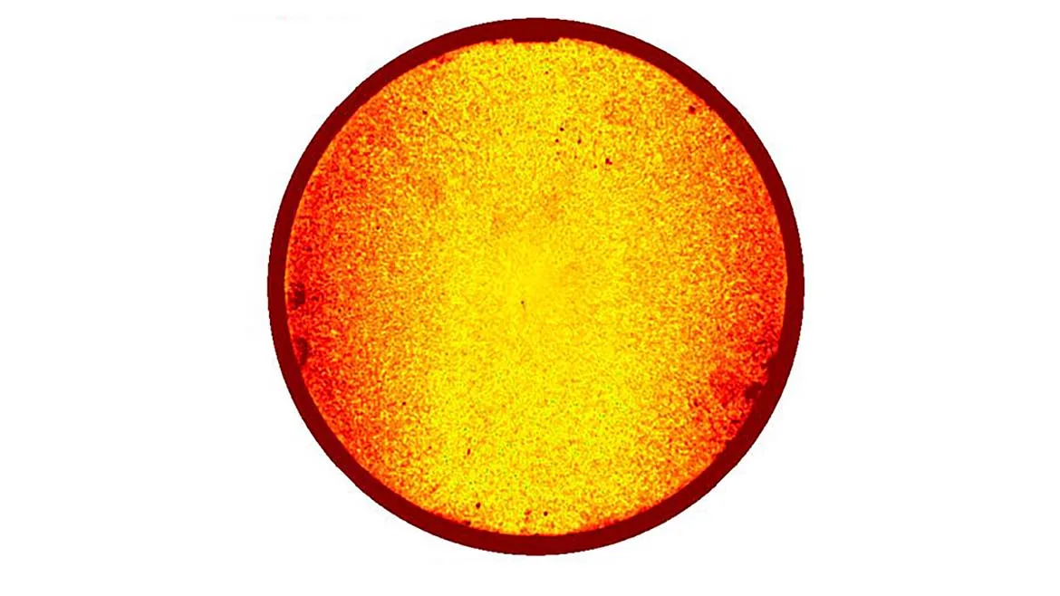
Example of a CMP Non-Polished Wafer
Electronics components are shrinking toward the nanometer scale. Yet the assemblies they inhabit, such as printed circuit boards (PCBs), probe cards, and multi-chip modules, are growing in complexity and physical footprint. As traditional contact-based measurement reaches its physical limits, 3D optical metrology has emerged as the new standard for maintaining high-yield production.
While confocal microscopy (CM) and white light interferometry (WLI) remain the gold standards for sub-nanometer roughness, many applications now require a larger measurement volume, necessitating a broader sensor portfolio.
Confocal Point (CP) Sensors: The "Optical Stylus"
The Confocal Point (CP) sensor embodies the precision of a traditional contour tool without physical contact. Instead, it uses a focused spot of light to measure surface profiles.
The sensor rasters across the surface to capture a linear profile, resets along the cross-travel axis, and steps forward to measure the next adjacent line. While these individual profiles can be stacked to create a highly accurate 3D area map, the tool offers immense flexibility. If a quality inspection task requires only a single 2D cross-section (X-axis versus height), the sensor can capture just that, saving valuable cycle time.
This capability expands the horizontal XY scale and the field of view. A traditional microscope is often limited to a narrow field of view spanning a few millimeters; a CP sensor can handle macro-scale parts ranging from 5 mm to 500 mm.
This scalability is well suited to complex assemblies or subassemblies, such as PCBs, switches, and connectors. Using dedicated automation software along with CP technology offers the flexibility to automate tens to thousands of individual profile measurements across these larger assemblies.
The software directly integrates with the factory’s statistical process control (SPC) software, feeding real-time dimensional data into the quality management system for instant analysis.
Confocal Line (CL) Sensors: Scaling for Speed
While CP sensors excel at flexible, large-scale profiling, they introduce a trade-off when a single point is too slow for production throughput and a full 3D surface mapping is required over large areas. Stacking thousands of individual point profiles to build a 3D image of a large component takes time. Mapping a 12-inch-by-12-inch component line by line could easily take an hour or two on the production floor.
This is where confocal line (CL) sensors shine. CL sensors project a linear array of light containing several hundred to 2,000 individual measurement points, scanning simultaneously in a single pass. In a single high-speed scan, the CL sensor captures a "band" or stripe of 3D data anywhere from 0.5 mm to 5 mm wide. This enables high-resolution 3D imaging of large surface areas in a fraction of the time required by CP sensors.
This changes how manufacturers approach quality control for complex, high-density components, including:
Ball Grid Arrays (BGAs) and Micro-BGAs: In a BGA, tiny soldered bumps act as the prongs connecting a microchip to a printed circuit board. These arrays can contain a few hundred to tens of thousands of miniature solder balls. To prevent connection failures, quality teams must ensure that every ball is present, perfectly positioned in the XY axis, and uniform in height. If a single ball is missing, misplaced, or at the wrong height (coplanarity), the chip won’t snap into place correctly, and the connection will fail. The CL sensor can sweep across these massive arrays in seconds, instantly verifying coplanarity and placement, preventing "open" or "short" circuits before the chip is even seated.
Probe Card Testers: A probe card is a specialized fixture used to test the matching contact pads on a circuit board or silicon wafer. It features ultra-dense arrays of tens of thousands of microscopic needles, or chisel-like tips, that are placed onto the pads to run electrical checks.
Because probe cards can be massive, frequently 400 mm × 400 mm or up to two feet square, inspecting the test fixture itself is a major quality challenge.
CL sensors can scan the entire needle array in wide, high-speed sweeps, mapping the height, alignment, and position of each micro-needle to ensure the tester interfaces correctly with production chips. If even one needle is slightly bent or out of spec, it will miss its corresponding contact pad, leading to costly failures or permanent damage to a sub-assembly.
The Non-Contact Imperative
For applications like probe card testing, non-contact optical metrology is the only viable option. The microscopic testing needles are incredibly fragile; touching them with a physical stylus would instantly bend, break, or misalign the components.
Furthermore, programming a point sensor to physically stop and measure tens of thousands of individual needles is impractical.
CL sensors deliver the rapid, non-contact 3D inspection required to keep pace with production.
High-Speed Confocal Line Sensors: The Cutting Edge of Throughput
For the highest-volume manufacturing environments, high-speed CL sensors represent the next generation of at-line metrology. By prioritizing rapid data acquisition, these optical sensors improve throughput by nearly an order of magnitude, a factor of 10. They enable quality teams to measure a complex assembly in minutes instead of hours.
To put this into perspective, consider the cycle times for inspecting a large component like a 400 mm × 400 mm probe card or a high-density PCB:
- CP Sensors: Can take several hours due to the time required to physically raster thousands of individual lines.
- Standard CL Sensors: Reduce the inspection time to roughly 30 minutes by capturing data in wider bands.
- High-Speed CL Sensors: Eliminate the production bottleneck, reducing the final cycle time to 5–10 minutes.
High-speed CL sensors are engineered specifically to maintain extreme measurement stability on the production floor. They achieve an impressive 50 nm axial (depth) resolution, along with lateral resolutions of 0.5 µm to 2.5 µm. Furthermore, because these sensors feature a high-aperture objective lens, they can accurately measure steep surface angles up to 53°.
This offers a significant advantage for micro-electronics applications such as bump inspection. Because solder bumps and BGA components are spherical, standard optical sensors often suffer from data dropouts at the steep, curved edges of the balls, where light scatters. By capturing reflections at angles up to 53°, high-speed CL sensors ensure exceptional data stability and completeness, delivering rapid, high-fidelity 3D mapping for high-volume electronics lines.
From Performance Testing to Process Control
Electronics manufacturers have historically accepted a level of "attrition" as the cost of doing business. Under this model, production relies strictly on performance-based testing. If a part didn't work during a final functional test, it was scrapped.
This approach creates an expensive blind spot by ignoring the why behind a failure. Consider a standard final test using a probe card fixture. If the tester fails to read a specific circuit patch, the system flags the part as defective. Because there is no data to prove otherwise, manufacturers assume the circuit is bad and scrap the entire board.
In reality, that circuit might be flawless; the failure was caused by a misaligned, bent, or worn needle that failed to make physical contact. Without optical metrology, manufacturers end up throwing away high-value components due to a lack of traceability.
Shifting the Quality Workflow
Integrating 3D optical metrology into the production line allows manufacturers to pivot from defensive attrition to proactive statistical process control (SPC). Automated optical tools provide an exact physical map of the assembly, yielding significant operational advantages:
- Eliminate Scrappage: Validating the physical integrity of the electronic assembly and test fixtures can immediately differentiate between a true product defect and a bad test connection. This rescues "good" circuits that would otherwise be discarded.
- Identify Trends: Instead of waiting for a part to fail a functional test, 3D optical data tracks microscopic drift in component height, solder volume, or XY positioning. Quality teams can see when a process is drifting out of tolerance and correct it before it creates scrap.
- Automated Integration: Modern 3D optical sensors are highly automated and easy to deploy at-line. They eliminate operator error while feeding dimensional data into SPC software in real time.
The transition to 3D optical metrology transforms quality control from a reactive, go/no-go process into an automated, cost-saving engine on the production floor. By moving beyond performance testing and embracing a high-speed, non-contact 3D workflow, manufacturers can ensure that as their products get smaller and more complex, quality and profitability continue to grow.
Next Steps
Successfully navigating this transition comes down to balancing several core variables:
- Application & Resolution Requirements: Begin by mapping the components’ specific microgeometry. While high-volume PCB assemblies, BGAs, and probe cards are drivers of this technology, the same optical toolkit is critical for inspecting ultra-precise microelectromechanical systems (MEMS) and micro-optical-electromechanical systems (MOEMS). The question is scale: does it require nanometer-level vertical resolution on an isolated micro-component, or a massive 500 mm horizontal XY scale?
- Throughput Analysis: How many parts per hour must be inspected, and where will the tool live? The choice of technology dictates whether a solution is optimized for an R&D lab, a standard factory floor, or a strict cleanroom environment.
The Selection Framework
When evaluating the right tool for a specific workflow, a general rule of thumb applies to the selection process:
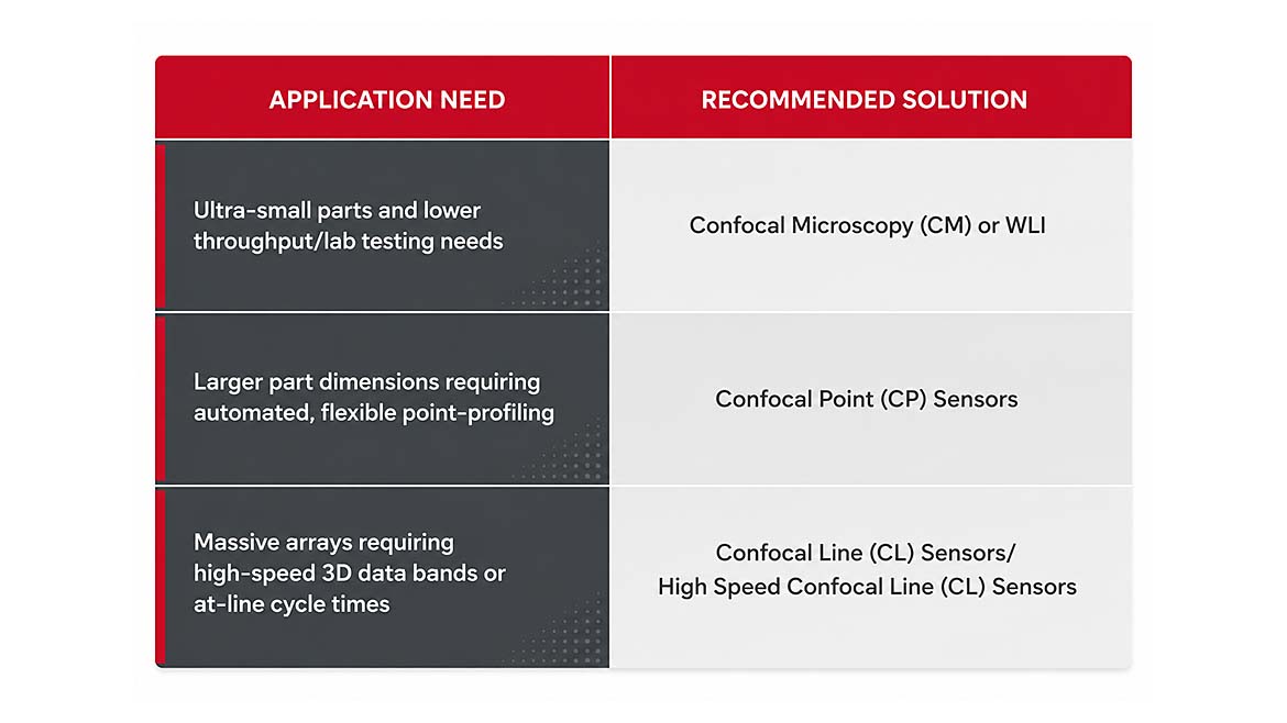
Source: Mahr
By matching the optical sensor to throughput and geometric needs, manufacturers can successfully move advanced optical tools out of the lab and into fully automated, high-yield production workflows.
Choosing the Right Partner
A sensor optimized for measuring sub-nanometer roughness of a MEMS device will be too slow to keep pace with a high-volume BGA assembly line. Conversely, a high-speed line sensor designed for production throughput won’t provide the specialized lateral resolution needed for deep R&D analysis.
Partnering with a metrology scientist to look at your specific microgeometries, surface materials, and cycle-time constraints allows you to evaluate the entire technology spectrum—including CM, WLI, CP, CL, and High-Speed CL—to find the most cost-effective path to 100% yield.
A partner that offers a comprehensive portfolio across the metrology spectrum, ranging from traditional contact stylus tools and standard confocal systems to advanced, cutting-edge point and high-speed CL sensors, can assess your exact tolerances and throughput targets without bias.
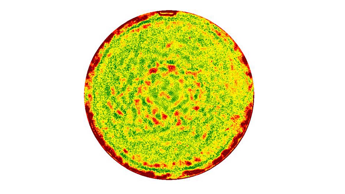
Example of a CMP Polished Wafer. Source: Mahr
Looking for a reprint of this article?
From high-res PDFs to custom plaques, order your copy today!