Vision & Sensors | Machine Vision
Maximizing Throughput, Minimizing Defects: Advanced Vision Technology for Efficient Wafer Inspection
Achieve reliable detection of macro defects with fast line-scan cameras and optimized lighting

This article addresses the critical challenge of efficient wafer inspection in semiconductor manufacturing, where maximizing throughput while minimizing defects is essential for production yield and cost efficiency.
Modern semiconductor production demands inspection methods that balance high-speed processing with exceptional defect detection sensitivity. Advanced machine vision technology is the key solution for reliable macro defect detection throughout the wafer production lifecycle - from bare substrates to finished components. Particles, contamination, scratches, and coating irregularities will significantly impact wafer quality and must be detected early to avoid costly downstream processing of defective components.
Challenges in Semiconductor Production
Developments in the field of electronic components continue to progress rapidly. The market and consumers demand features such as the miniaturization of products while increasing performance. At the same time, these advancements are expected to come with ever lower energy consumption.
These trends lead to increasingly complex challenges for manufacturers of semiconductor components on two levels. On the technical side, ever-smaller components and structures, combined with higher production speeds, require extreme precision in manufacturing accuracy. At the same time, semiconductor manufacturers must keep a close eye on the cost-efficiency of their processes to remain competitive. Their goal must be to maintain low error rates and produce as little waste as possible.
Hiring more or better-trained personnel is generally not a sustainable solution: skilled workers are hard to find and expensive to keep. Additionally, humans are more error-prone than automated processes. These challenges can therefore only be addressed through the intensive use of high-performance automation systems. In this context, machine vision plays a critical role in quality control.
Machine Vision for Macro Defect Detection
Anyone aiming to manufacture wafers cost-effectively must ensure high yield in production. It is therefore essential to detect yield-reducing defects as early as possible in order to adapt further processing and avoid unnecessary cost from performing production steps on already defective components. Wafers are inspected at many stages—from the bare wafer substrate to the final component — for deviations from defined quality standards.
One important category of potential defects in semiconductor components includes so-called macro defects. Macro defects can manifest in various forms, which can be difficult to detect and classify. They can occur on bare wafers, on the back of a wafer, but also as irregularities on structured or coated wafers.

Some examples for macro defects are particles or contaminations as well as surface scratches. Faulty processes during the chemical mechanical polishing can result in scratches, residues or unpolished areas. Monitoring of the etching process must be done to look for residues, corrosion, or pattern flaws.
Large area defects such as coating irregularities, bad contacts or missing structures are further macro defects that need to be reliably identified. Features like coating integrity, cleanliness and surface quality are also details that need to be verified during outgoing quality control procedures.
Keeping up with the high volumes of wafer production requires fast and efficient inspection methods to maintain production rates. The detection methods used must also be sensitive enough to detect defects while minimizing false positives and negatives, which can be a delicate balance to achieve. Wafers must be handled and readied for inspection with great care to avoid further damage or faults that unnecessarily complicate the process.
Machine vision systems play a crucial role in reliably detecting such macro defects. When properly selected and implemented, these systems can keep pace with high production speeds and identify defects with high accuracy. The demands on quality inspection and control require the entire wafer to be examined at high resolution and within a short time frame.

Application Specific Requirements: Cameras
The decisive component of a vision system is the camera used. Ideally, all macro defects on wafers can be captured with a single camera system. This leads to the following basic camera requirements:
- Scan width: 300 mm are a common size for today’s wafers. Cameras with a scan width of more than 300 mm are therefore useful to cover full 300 mm wafers.
- Speed: A scan time of less than 10 seconds per 300 mm wafer should be possible in order to meet the requirements for economical production processes.
- High resolution: To aim for high quality, typically defects in the range from 5 µm to 15 µm need to be detectable.
- Color capturing: Detecting coating irregularities requires color cameras.
Line-scan cameras have proven particularly effective in high-speed processes where even minor defects must be detected. With this technology, images are captured line by line and then assembled or “stitched” into a complete image. This contrasts with area scan cameras that capture an entire grid of pixels in a single moment. This makes it possible to produce high-resolution images of wafers in a very short time, which serve as the basis for automatic detection of macro defects.
New generation CMOS line-scan sensors now offer a similar image quality as CCDs, coupled with additional benefits specific to CMOS technology such as higher readout speed and flexible readout modes. Unlike single-line CCDs, these sensors have several lines of pixels, allowing for different operation modes depending on an application’s requirements. One key benefit of a multiline sensor is the time delay integration (TDI) option. TDI consists of adding up the values of adjacent pixel lines synchronously with the motion of the object below the camera. The same section of the object is imaged by several lines, and adding up the signals of all these lines increases the signal intensity compared with a single line sensor. This solution has a much better signal-to-noise ratio than an equal increase in gain.
Advantages of line-scan cameras for wafer inspection are:
- • They offer a cost-efficient solution for high resolution imaging.
- • High line-scan rates allow for high transport speeds.
- • Using line-scan cameras ensures that the angle of illumination is exactly aligned and adjusted.
- • Compared to area scan cameras, line-scan systems deliver better light homogeneity.
- • Line-scan cameras reduce the image distortion to just one dimension.
- • Line-scan cameras with trilinear sensors improve the resolution by acquiring three color samples per pixel.
- • Multi-field imaging based upon line-scan cameras permit multiple images in one pass, thus saving cost and time.
Application Specific Requirements: Illumination
The quality of line-scan images also depends on the selected illumination. To capture images with sufficient contrast at high acquisition speeds, you’ll need both high light intensity and the most uniform illumination. In addition, different types of light are needed to detect different kinds of macro defects. Therefore, when selecting line lighting, it must be ensured that appropriate bright-field, dark-field, or coaxial lighting is used, depending on the application, to clearly highlight any defects.
Selecting the right illumination for a macro defect detection system takes experience and a high level of expertise. Some of the criteria for optimal selection are:
- • Depending on the application, a combination of different lights might be the perfect solution to detect different defects.
- • The type of macro defect is crucial when choosing the color of the illumination. Devices with different colored light can be the foundation of efficient solutions.
- • High-speed processes require illuminations with extreme intensity to acquire images with meaningful data.
- • High homogeneity of the selected illumination is a key prerequisite for reliable results.
To capture the complete geometry of a 300 mm wafer at high resolution and fully cover a field of view of this size, multiple cameras arranged side by side may be necessary. Modern innovation allows direct synchronization between multiple line-scan cameras, resulting in perfectly aligned composite images from the cameras, simplifying subsequent image processing.
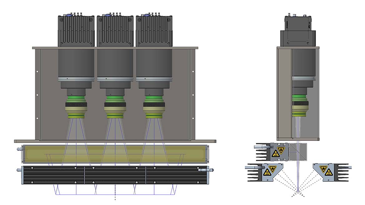
Another unique feature of modern line-scan cameras is their multi-field imaging capability. This technology leverages an integrated multi-channel flash controller to synchronize up to four light sources with the camera’s line trigger in a rapid sequence. Consequently, up to four images are captured in a single pass, each taken under different lighting conditions. This approach reduces the number of cameras installed, simplifying the inspection process, and contributing to the overall optimization of process cost.
Customized Systems
Given the uniqueness of various fabrication processes, a customized system is often the answer. This includes careful selection of line-scan cameras, optics, lighting and various accessories. Available installation space and operational simplicity are two other factors to think about. The customized approach results in systems that meet exacting requirements yet remain cost optimized. A custom system should also be pre-adjusted and 100% tested, so it can be installed in a machine with minimal effort and risk.
Conclusion
Electronic components form the basis of virtually every product used in daily life. Vehicles of all kinds, communication devices, energy generation, data processing, and the entire consumer electronics sector are just a few of the countless segments that would be unimaginable today without powerful semiconductors.
With global sales of $627–$630 billion (USD) in 2024, the semiconductor industry is a huge and quickly expanding sector driven by demand for consumer electronics, AI chips, and other cutting-edge technologies. To continue to thrive in this highly competitive environment, manufacturers must produce semiconductors efficiently by optimizing every step in the process with accurate inspections. Because of the minute structures involved, optical inspection in modern semiconductor manufacturing now occurs in the micrometer range. The need to detect defects and contaminations at this scale places the highest demands on inspection systems. Extremely high-resolution line scan cameras can capture these minute structures at high speeds for image analysis.
Looking for a reprint of this article?
From high-res PDFs to custom plaques, order your copy today!


